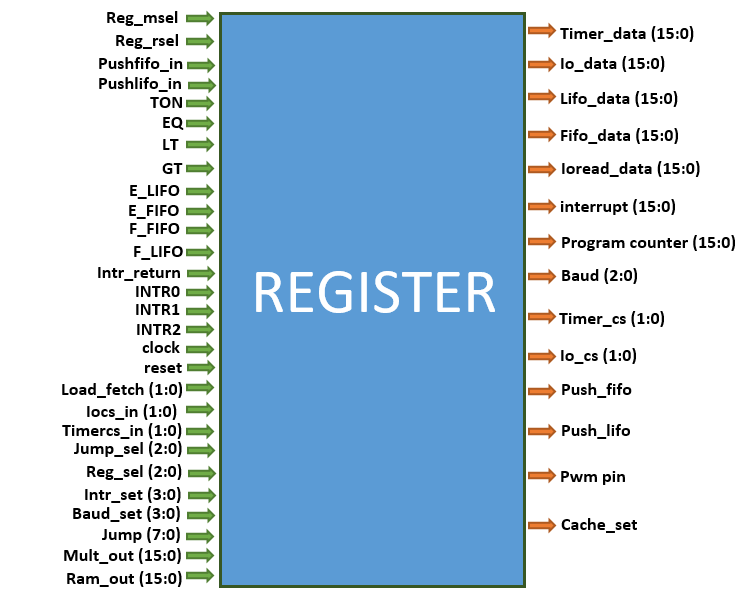
10.1 Why do we need the registers? The cpu has two major data storage units. The registers and the memory which is an array of registers. Whenever the cpu has a need to store data, whether after an arithmetic or logical operation, fifo data, lifo data etc. The data has to be stored either in the memory or register. The memory is usually required when they are large number of data to be stored or unknown number of data to be stored. Data stored in memory would usually require an address to access them and they are usually slower. One obvious reason for this is that, to access data in memory requires atleast one clock cycle while data in registers are accessed instantly but memory are usually larger in size compared to registers. When a design requires storage of a finite small size of data example the output of an alu operation, 16-bit control signal, currently decoded instruction and not all of the instruction, data bus output etc. These finite small number of data are best stored in the registers and they are instantly accessed when needed which makes them faster than memory.
10.2 The register unit
The Register unit is optimized for the IOSOC Enhanced RISC instruction set and consist of fourteen 16-bit registers.
7 registers are directly accessed by the ALU and can be operated on, in one clock cycle. They include:
1. Timer data register
2. Input/output write register
3. Fifo register
4. Lifo register
5. Input/Output read register
6. Program counter register
7. Interrupt register
Each of the sub units can access these registers only if their chip enable pin is set else they are used as general purpose registers. Not all of the registers can be accessed through the chip enable pin. The IO READ register does not have a chip enable and therefore, continously sends read data to the IO port. The interrupt register only has a intr signal which is used to load the interrupt control data registers. Depending on the value of the Intr signal, the interrupt register can only load its data to the control register. The program counter register should not be used as a general purpose register only address of instruction to be fetched should be stored here. The baud register stores the baudrate signal for the UART. To set the baudrate, when the bit0 of the baud_set signal is equal to ‘1’ the cache_set
signal is turned on, indicating a UART operation and when it is low, it indicates a FIFO operation. This cache_set signal switches between using
the Cache unit as an UART or a FIFO. So, when the bit0 of the baud_set signal is equal to ‘1’, bit(3 downto 1) of the baud_set
signal is loaded to the baud register.
The system has three hardware interrupts (INTR0, INTR1, INTR2) which are connected on three separate pins that are not connected to the I/O ports.
The interrupt and pwm control registers includes:
1. Interrupt register
2. Interrupt return register
3. Interrupt data0 register
4. Interrupt data1 register
5. Interrupt data2 register
6. frequency control register
7. Interrupt set0 register
8. Interrupt set1 register
9. Interrupt set2 register
10. pwm set register
The interrupt register is the main register that feeds data to the interrupt and pwm control registers using the intr signal. It can also serve as a genera purpose register when the intr signal is set to zero. When an interrupt occur, the interrupt return registers stores the address of the next instruction until after the interrupt. After the interrupt instructions has been executed if the interrupt return signal is triggered then the interrupt return register releases the address to the program counter. The interrupt data0 register, interrupt data1 register, interrupt data2 register stores the address of the interrupt. In a case where any of the interrupt is triggered the address stored in its data registered is executed. The frequency control register stores the count for the pwm. The interrupt set0 register, interrupt set1 register, interrupt set2 register is used to enable or disable the interrupt. The Pwm set register is also used to enable the pwm pin. All the interrupt control register are modified with the intr signal.
10.3 The Pinout
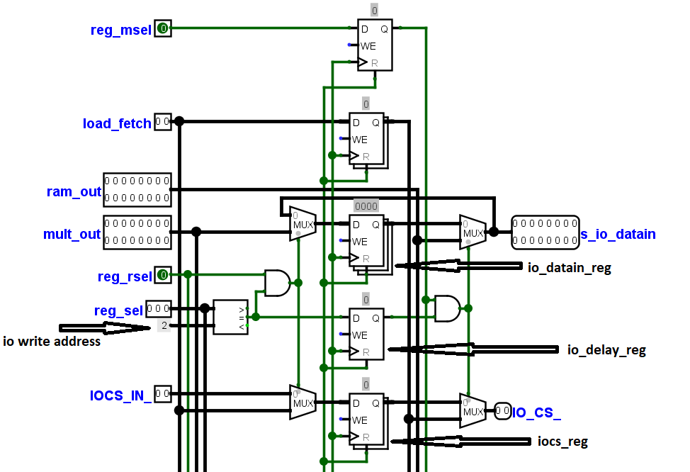
The RAM_OUT and the MULT_OUT are the two major data input signals to the register unit.
The RAM_OUT signal holds input from the ram while the MULT_OUT holds input from registers.
Fetching data from memory takes an extra clock cycle compared to fetching data from registers. This usually makes memory fetch instructions to take more cycles in most CPU designs.
Here, the model has been designed to integrate both data from memory and data from register to arrive at the same time .
This makes both memory fetch and register fetch to take one clock cycle . The HDL code will explain how this integration was achieved.
The reg_mselsignal indicates that the data is coming from memory while reg_rsel signal indicates that data is coming from register.
The reg_sel signal holds the address of the register where data is to be stored. Typically values ranges from 1 – 7.
During a ‘load to register’ instruction, two extra bits called the load_fetch signal acts as the chip_enable or chip_select .
This signal determines if the data to be loaded to the register should be sent to its sub unit or serve as a general purpose register (temporary storage for other registers,
memory or for ALU operation). If data are not sent to the sub units using the load_fetch signal during a ‘load to register’ instruction ,
it can also be sent directly using the: PUSHFIFO_IN (from the fifo register to the cache unit), PUSHLIFO_IN
(from the Lifo register to the Lifo unit), IOCS_IN ( from the io_datain register to the i/o write input ), TIMERCS_IN
(from the timer register to the timer unit). The ioread register is directly connected to the i/o read input at the i/o unit.
Therefore it should not be used as a general purpose register.
This Brainio has seven feedback signals that can be used to interrupt the program :
F_LIFO (the stack is full), F_FIFO (the cache is full), E_FIFO (the cache is empty), E_LIFO (the stack is empty).
These signals reads the state of the cache and stack. GT (greater than), LT (Less than), ET (Equal to).
These signal reads the state of an ALU computation. The feedback signals are used to prompt a jump interrupt .
The number of instructions to jump can either be incremented or decremented and this value is stored in the JUMP signal.
The TON signal is used to initiate a delay interrupt and would be used for a software program that initiates a delay.
This signal achieves this by preventing the program counter from incrementing, Making it to repeat a particular instruction throughout the period of the delay.
The timer unit is used to synchronize this signal.
The intr_return signal marks the end of an hardware and commands the program counter to return to the last instruction before the interrupt.
INTR0, INTR1 , INTR2 are the hardware interrupt pins.
The intr_set signal is used to turn on/off the interrupt pins i.e to enable or disable the interrupt pin.
It also selects which interrupt data register to store the data from the interrupt register. Finally, the baud_set
signal is used to set the baud rate for an UART operation.
The output of the register unit consist of the seven general purpose register .
Next is their chip_select : timer_cs, io_cs, push_fifo, push_lifo . The interrupt_register does not have an external chip_select,
rather the intr_set signal sets which interrupt data register to store its data. With a value of zero on the intr_set signal ,
no data is stored and the interrupt_register can serve as a general purpose register .Also the chip_select for the program counter
is within the unit and not shown external. The IO_READ register does not have a chip select,
this register is connected directly to the i/o read input. Care should be taken if used as a general purpose register.
The freq_pin produces the PWM signal. baudsignals selects the baud rate for an UART operation.
The cache_set signal if high, sets the cache unit as an UART , and if low , sets the cache unit as a FIFO.
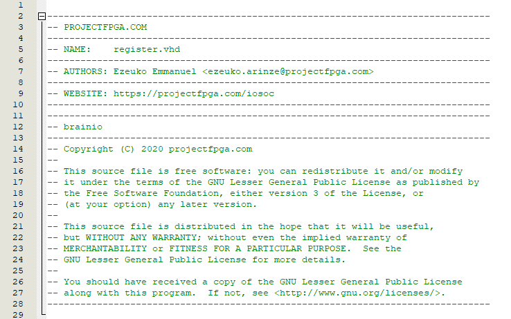
10.4 register.vhd
First, we introduce the introduce the title.
Next we include the IEEE; library.
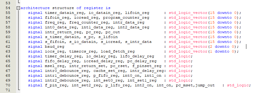
The port consist of all the pinouts in the diagram above.
Next are the signals which we would explain next.
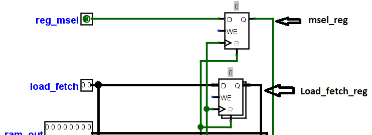
As explained earlier, reading data from memory takes one cycle delay. Therefore, to write from memory to a register we need to wait one cycle. Therefore, we would wait for the memory by delaying the LOAD_FETCH signal which is used for chip select and also the REG_MSEL signal which indicates we are writing from memory. The new signals after the delay would be load_fetch_reg and msel_reg respectively.
During a write from memory, if the REG_SEL matches the address of a particular register, then it is also delayed. The delayed signal is the register_delay_reg. During a write from register, the REG_SEL matches the address of the register and the REG_RSEL is also enabled.
Timer signals
Definitions
timercs_reg
timer chip select register
TIMER_CS
timer chip select output
TIMER_CSIN
timer chip select input without a write from register or memory
LOAD_FETCH
timer chip select input during a write from register
load_fetch_reg
Delayed LOAD_FETCH and timer chip select input during a write from memory.
REG_SEL
holds the register address. ‘001’ is the timer register address during a write from register
timer_delay_reg
Delayed REG_SEL. Timer register address during a write from memory.
msel_reg
Delayed REG_MSEL. Write from memory select.
REG_RSEL
Write from register select.
MULT_OUT
Timer register data, during a write from register.
RAM_OUT
Timer register data, during a write from memory.
s_timer_datain
Timer data output
timer_datain_reg
Timer register during a write from register
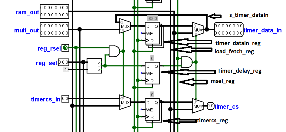
For the timer register. During a write from memory. The REG_SEL is equal to ‘001’ which selects the timer register and REG_MSEL is high. These two signals are delayed to give two new signals: timer_delay_reg and msel_reg. The s_timer_datain and TIMER_CS will take the value of the RAM_OUT and load_fetch_reg else they take the value timer_datain_reg and timercs_reg. During a write from register, the REG_SEL is equal to ‘001’ which selects the timer register. Then the timer_delay_register is set to 1 on the next clock cycle. If the REG_RSEL is high, then it is a write from register. The timer_datain_reg and timercs_reg takes the value of the MULT_OUT and LOAD_FETCH respectively. If it is not a write from register the timer chip select selects the value of TIMER_CSIN. If the timer is not selected then the timer register would latch with the s_timer_datain.
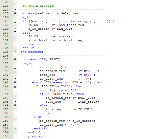
IO write
Definitions
iocs_reg
IO write chip select register
IO_CS
IO write chip select output
IO_CSIN
IO write chip select input without a write from register or memory
io_delay_reg
Delayed REG_SEL. IO write register address (‘010’) during a write from memory.
s_io_datain
IO write data output
io_datain_reg
IO write register during a write from register
During a write from memory, the s_io_datain and IO_CS stores the RAM_OUT and load_fetch_reg data respectively when the msel_reg and io_delay_reg is equal to one . During a write from register the io_datain_reg and the iocs_reg are used to store the MULTOUT and the LOAD_FETCH respectively when the REG_RSEL is equal to one and REG_SEL is equal to ‘010’. When the IO write register is idle, the io_datain_reg latches with the s_io_datain while the IO_CSIN is continuously input to the iocs_reg.
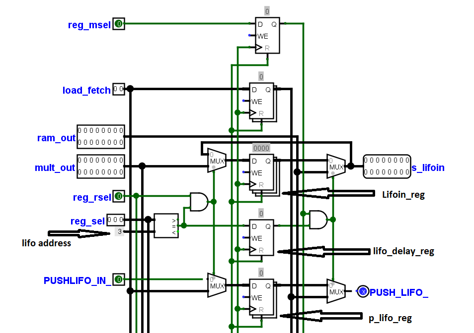
LIFO signals
Definitions
p_lifo_reg
LIFO chip select register
PUSH_LIFO
LIFO chip select output
PUSHLIFO_IN
LIFO chip select input without a write from register or memory
lifo_delay_reg
Delayed REG_SEL. IO write register address (‘011’) during a write from memory.
s_lifoin
LIFO data output
lifoin_reg
LIFO register during a write from register
During a write from memory, the s_lifoin and PUSH_LIFO stores the RAM_OUT and load_fetch_reg data respectively when the msel_reg and lifo_delay_reg is equal to one . During a write from register the lifoin_reg and the p_lifo_reg are used to store the MULTOUT and the LOAD_FETCH respectively when the REG_RSEL is equal to one and REG_SEL is equal to ‘011’. When the LIFO register is idle, the lifoin_reg latches with the s_lifoin while the PUSHLIFO_IN is continuously input to the p_lifo_reg.
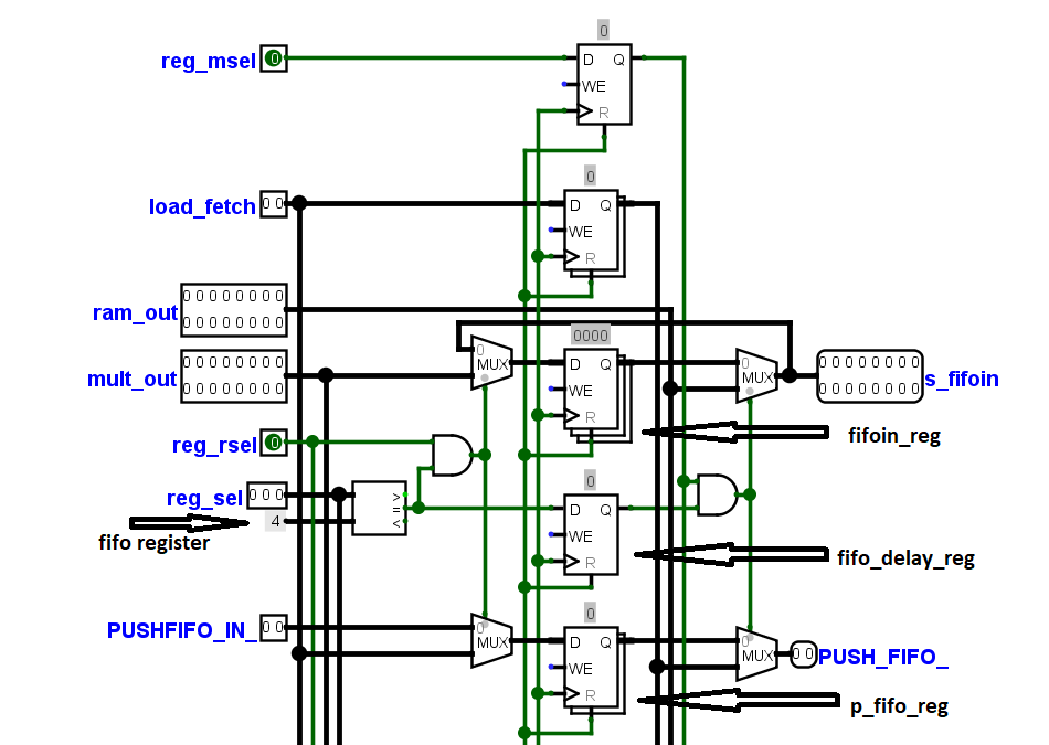
FIFO signals
Definitions
p_fifo_reg
FIFO chip select register
PUSH_FIFO
FIFO chip select output
PUSHFIFO_IN
FIFO chip select input without a write from register or memory
fifo_delay_reg
Delayed REG_SEL. IO write register address (‘011’) during a write from memory.
s_fifoin
FIFO data output
fifoin_reg
FIFO register during a write from register
During a write from memory, the s_fifoin and PUSH_FIFO stores the RAM_OUT and load_fetch_reg data respectively when the msel_reg and fifo_delay_reg is equal to one . During a write from register the fifoin_reg and the p_fifo_reg are used to store the MULTOUT and the LOAD_FETCH respectively when the REG_RSEL is equal to one and REG_SEL is equal to ‘011’. When the FIFO register is idle, the fifoin_reg latches with the s_fifoin while the PUSHFIFO_IN is continuously input to the p_fifo_reg.
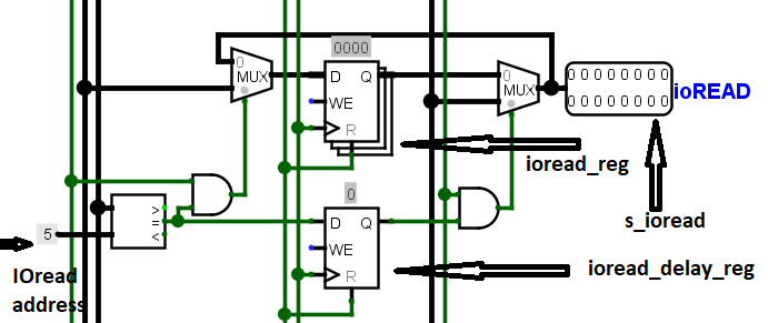
IO READ signals
Definitions
ioread_delay_reg
Delayed REG_SEL. IO write register address (‘101’) during a write from memory.
s_ioread
IO READ data output
ioread_reg
IO READ register during a write from register
During a write from memory, the s_ioread stores the RAM_OUT when the msel_reg and ioread_delay_reg is equal to one . During a write from register the ioread_reg is used to store the MULTOUT when the REG_RSEL is equal to one and REG_SEL is equal to ‘101’. When the IO READ register is idle, the ioread_reg latches with the s_ioread.
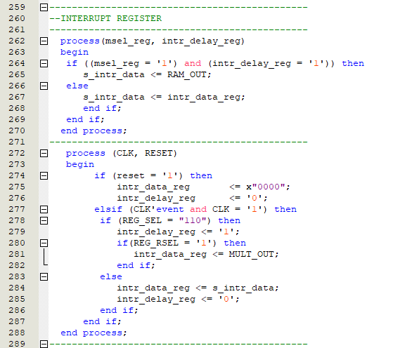
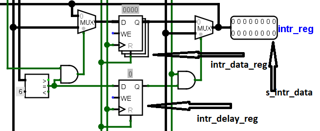
Interrupt signal
Definitions
intr_delay_reg
Delayed REG_SEL. IO write register address (‘110’) during a write from memory.
s_intr_data
interrupt register data output
intr_data_reg
Interrupt register during a write from register
During a write from memory, the s_intr_data stores the RAM_OUT when the msel_reg and intr_delay_reg is equal to one . During a write from register the intr_data_reg is used to store the MULTOUT when the REG_RSEL is equal to one and REG_SEL is equal to ‘110’. When the interrupt register is idle, the intr_data_reg latches with the s_intr_data.
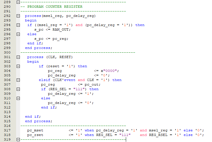
program counter
Definitions
pc_delay_reg
Delayed REG_SEL. IO write register address (‘111’) during a write from memory.
s_pc
program counter store
pc_reg
program counter register
During a write from memory, the s_pc stores the RAM_OUT when the msel_reg and pc_delay_reg is equal to one . During a write from register the pc_out is used to store the MULTOUT when the REG_RSEL is equal to one and REG_SEL is equal to ‘111’.
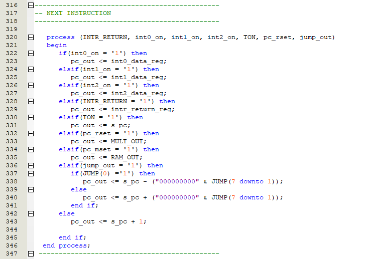
The output of the program counter is the pc_out. While the program counter fetches/increments the next instruction from the program memory, certain conditions can make it to jump to the address of certain instructions. Some of these conditions includes the intrerrupts which has the highest priority. They are int0_on, int1_on, int2_on. Next is the interrupt return bit0, this signals the end of an interrupt execution and tells the program counter to go back to the previous instruction it was executing. The previous instruction is stored in the intr_return_reg at the start of an interrupt. Next is the timer signal or TON which turns on if the timer is incrementing or decrementing, this signal stops the program counter from incrementing and assigns the next instruction as the previous instruction, this is used during a delay operation. Next is the pc_rset and pc_mset. These two signals are used during a register write and memory write respectively. That is, when the address of the next instruction is contained in register or memory. Finally, the jump_out signal, used when the instruction reads its feedback using an if statement example: if(fifo is empty){jump}, if(an alu operation is equal to zero){jump}, we would discuss all of them later. When the instructions reads this feedback and if the condition is true, it can jump to certain part of the instruction. Then, if no conditions are met the program counter would simply increment itself.
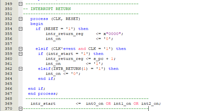
Initially, when an interrupt whether int0, int1 or int2 is turned on. The intr_return_reg stores the address of the next instruction it is supposed to execute before the interrupt and also the int_on signal comes on indicating that an interrupt is currently and prevents any other interrupt from overriding it. At the end of an interrupt execution, the INTR_RETURN signal is triggered. The INTR_RETURN bit0 sets the program counter to the instruction stored in the intr_return_reg while the INTR_RETURN bit1 sets the int_on signal back to zero enabling interrupts again.
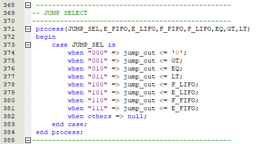
The feedback or jump conditions. The instruction can read the states of certain components and jump by incrementing or decrementing to a certain instruction based on if the condition is true or false. They include: ‘000’- Nothing, ’001’- (if registerA is greater than registerB){jump}, ’010’- (if registerA is equal to registerB){jump}, ’011’- (if registerA is less than registerB){jump}, ’100’- (if the lifo is full){jump}, ’101’- (if the lifo is empty){jump}, ’110’- (if the fifo is full){jump}, ’111’- (if the fifo is empty){jump}.
The simplest form of a debounce circuit is shown below. The output only turns on when the input was previously off and currently on. The output turns on when the input is currently off and was previously on. This type of simple debounce circuit is neccssary because the interrupts are directly connected to the program counter and incase of multiple reading of pins, it can cause error in the whole design. We would only use the debounce circuit to turn on the interrupt. Therefore, the debounce circuit is not necessary to turn it off because when the program has completely executed the interrupt instructions and the interrupt pin is still on, it can read it again without a need to know if it turned off initially, before coming on again. This debounce is shown on line 405, 406, 407, 426, 427, 428.
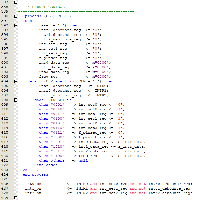
We need to set controls for the interrupt including which interrupt should be enabled or disabled, which instructions to execute when we receive an interrupt. Also, let us set control for the PWM pin including if it should be enabled or diabled, what count to use etc. Let us create a signal called INTR_SET to handle this. Different values of this signal changes different controls. int_set0_reg, int_set1_reg, int_set2_reg are used to enable interrupt 0, 1 and 2 when their value is 1 and also disable the three interrupts if their value is zero. f_pinset_reg is used to enable or disable the PWM pin. int0_data_reg, int1_data_reg, int2_data_reg stores the address of the instruction that marks the beginning of each interrupt when they are activated. The interrupt_return_signal marks the end of each interrupt. The freq_reg stores the number of counts for the pwm pin. The interrupt data registers and the pwm data register would take the value of the interrupt register when the INTR_SET activates them.
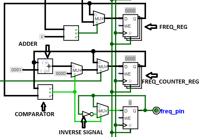
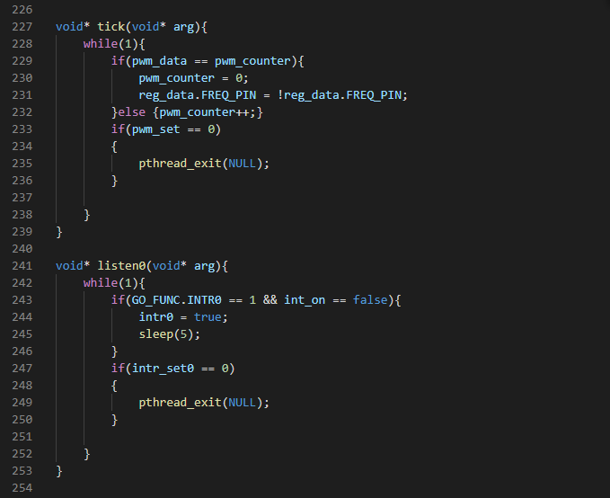
The simplest way to generate a pulse is given below. By generating the inverse signal per every steady count, we can generate a pulse.
If the f_pinset_reg is set then the pwm pin is enabled. The freq_counter_reg will keep counting or incrementing until it equals the value in the freq_reg then it resets, and the pwm_pin will take the value of its inverse signal.
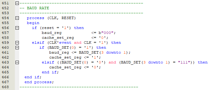
Let us set controls for the Cache, fifo and UART. We would use the BAUD_SET signal and the baud_reg signal is the baud rate of the UART transmission. If the BAUD_SET bit0 is equal to one, then we set the cache_set_reg to one which switches the cache for the UART transmissions and sets the baud rate of transmission to bit 3 downto 1. Else when bit0 of BAUD_SET is zero and bit 3 downto 1 is equal to ‘111’ then the cache_set_reg is set to zero which switches the cache to a FIFO.
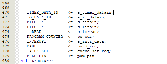
Finally, we assign the register signals to their respective outputs.
10.5 register.h
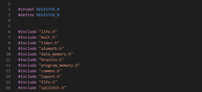
The register unit will include a lot of other sub unit header files to access their struct and functions. lifo.h- It will read the state of the lifo, if it is empty or full. fifo.h- It will read the state of the fifo, if it is empty or full. timer.h- It will read the state of the timer delay, if it is on then it will halt the program counter. alumath.h- It will read the output of an alu operation and store it in a register. data_memory.h-The output of the data memory will be stored in the register. brainio.h- the interrupt pins are temporary stored here, since we are not running it on an actual board. program_memory.h - we would be reading the next instruction from this memory. splitbit.h - we would be reading parts of an instruction.
Next we need to create the register struct which will include all the register outputs consisting of the registers to the other sub units including their chip select. Let us call it registers reg_data.
We would also create an ENUM which consist of the address of the registers.
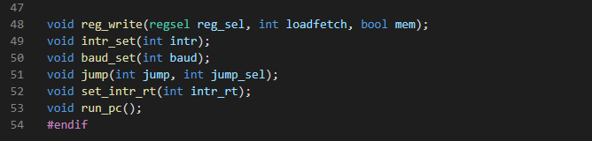
Finally, let us include the global functions: reg_write()- Used to write to a register. intr_set() - Used to set interrupt and PWM control signals. baud_set() - Used to set the FIFO unit. jump() - Used to jump to certain address in the program counter. set_intr_rt() - Used to set the return address after an interrupt. run_pc() - Used to fetch the next instruction.
10.6 register.c
The interrupt pins are steady listening for signals, so we will place them in a thread. Therefore, I have included the and . We will also include the register.h.
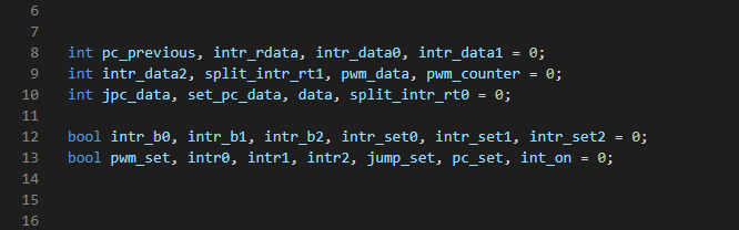
Next, the variable which we will explain later.
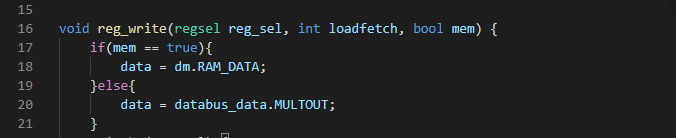
The register_write() is used to write data to the register. It will use three arguments. regsel called reg_sel which stores the address of the register we want to write data to, next is the loadfetch signal which contains the chip select of the selected register. Data can either be written from memory or register. Therefore the last argument bool mem will decide if the incoming data is from a register or the data memory. If the incoming data is from memory it will set the data to the output of the data memory called RAM_DATA which is the struct called dm else if the incoming data is from the register then the data will be set to the output of the databus called MULTOUT which is contained in the databus struct called databus_data.
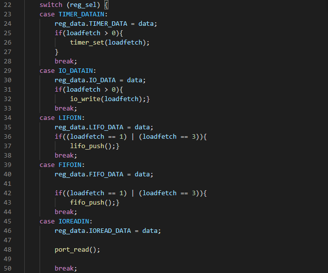
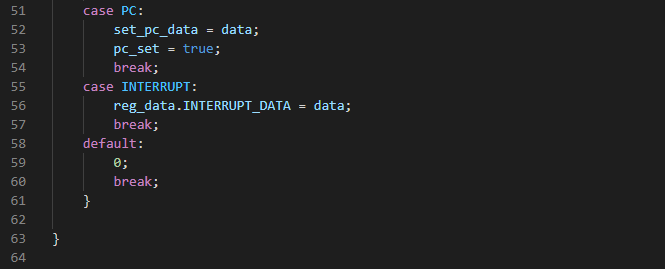
We would switch the register address, if it matches any of the register address in the ENUM we created, then we set the output of that register which is contained in the struct reg_data to the value of data. If the timer register is set and the loadfetch is greater than 0, then we set the timer unit using this signal. If the IO write is selected and the loadfetch is greater than zero, then we set the io_write using the loadfetch. If the lifo or fifo is selected and the loadfetch is equal to ‘01’ or ‘11’ then we push the lifo or fifo. If the IO READ is selected, then we call the port_read immediately. IF the Program counter is selected, the set_pc_data stores the data and the pc_set signal is set to true.
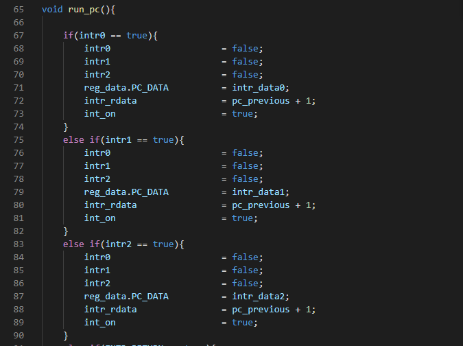
The run_pc() is used to set the next instruction. A lot of conditions would be used to determine the next instruction according priority. The highest priority is intr0. When any of the three interrupts are set, the next instruction which is called reg_data.PC_DATA (PC_DATA in reg_data struct) is set to the address of the interrupt data. The interrupt data include: intr_data0, intr_data1, intr_data2. Then the intr_rdata (interrupt return) will store the address of the next instruction before the interrupt was set. It will also disable the rest of the interrupts and set the int_on on. The int_on signal will ensure that no other interrupt comes on when an interrupt is currently being executed.
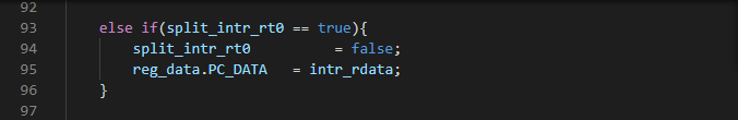
After an interrupt execution, if bit0 of the interrupt return signal is set , then we return the program counter to the address in the interrupt return register.
If the timer delay is on, then we delay the program counter by setting its value to the initial instruction, when the timer has completed then we can increment it. The program actually halts at the timer unit when during the delay count, so this part never really gets executed except when we put the timer counter in a thread which we would do in a later version of this course.
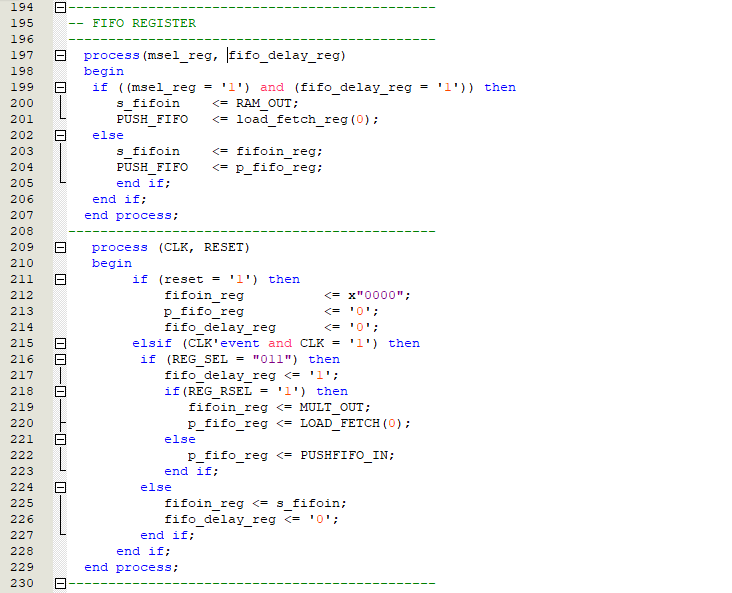
If the pc_set signal is set , that is when the pc register has a data to execute. The next instruction becomes the value in the set_pc_data and this pc_set signal is disabled.
If a jump is set , then the next instruction becomes the jmp_pc_data and this signal is set to zero.
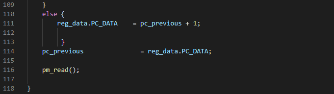
In the absence of any condition, the program counter would increment its previous value and set the previous value to its new value. And finally, call the pm_read(). This function reads the next instruction from the program memory.
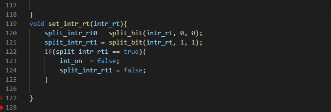
At the end of an interrupt execution, the set_intr_rt() is triggered. Bit0 of the intr_rt signal is used to return the program counter while bit1 is used to turn off the int_on signal and allow a new interrupt.
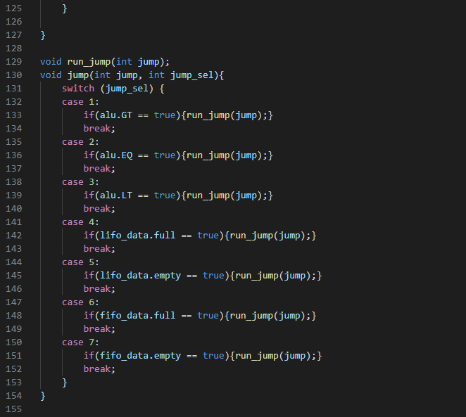
The feedback or jump conditions. The instruction can read the states of certain components and jump by incrementing or decrementing to a certain instruction based on if the condition is true or false. The case statement is used to switch the jump_sel argument. They include: ‘000’- Nothing, ’001’- (if registerA is greater than registerB){jump}, ’010’- (if registerA is equal to registerB){jump}, ’011’- (if registerA is less than registerB){jump}, ’100’- (if the lifo is full){jump}, ’101’- (if the lifo is empty){jump}, ’110’- (if the fifo is full){jump}, ’111’- (if the fifo is empty){jump}.
The jump condition if true will trigger the rum_jump(). It argument is the jump which is the number of steps to increment or decrement. Bit0 of the jump argument will determine whether to increment or decrement. The jump_set is set to true which tells the program counter that a jump is available.
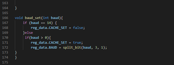
I previously designed the UART in VHDL in a previous course in udemy which I have used as part of the cache unit in VHDL. But in C, I ignored the UART since I haven’t developed the C version of the UART. Rather the cache unit is a single FIFO, while in VHDL the cache unit can be switched between a single FIFO or an UART with two FIFO. 14 in binary is ‘1110’. If bit0 of the baud is zero and bit 3 downto 1 is equal to ‘111’, then the CACHE_SET is turned off which turns the cache to a single fifo. Else if bit0 is equal to one then CACHE_SET is turned on which sets the cache unit to a UART and thE 3 downto 1 is used as the baudrate of transmission. This particular code block is redundant since there is no C version of the UART and the cache is just a single fifo. The UART will be added in a later version of Brainio.
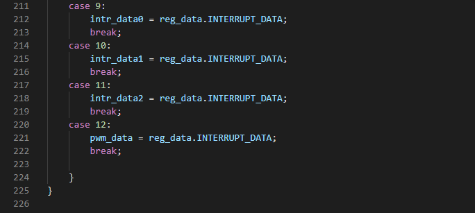
We also need to set the interrupt controls using the intr_set(). This function has one argument, intr. intr_set0, intr_set1, intr_set2, are used to disable or enable the interrupts. These signals also set the int_start() which is a thread that continuously listens for interrupt. The intr_set() also sets the pwm pin that triggers the start_clock() which is also a thread. The intr_data0, intr_data1, intr_data2, pwm_data stores the interrupt data instruction and the pwm number of counts. These signals are initially stored in the interrupt register until when the intr argument selects them.
Below is the interrupt code for both the int_start() and the start_clock(). This requires good knowledge of C thread.