5.4 datamemory.vhd
First let us declare the title.
Next is the IEEE; standard library
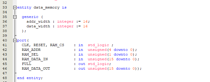
On line
33 we declare the entity called
data_memory. The generic contains the ram address size and data width size. Both the data width and address size are 16-bit wide.
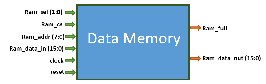
The port consists of data pins discussed in the diagram above.
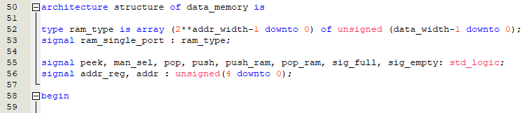
next we declare the architecture which consists of the signals and ram which we will discuss as we go through the code.
We define the
RAM_SEL input single. Depending on what value it is, its output can either be:
peek-(use the address on the
RAM_ADDR input, and do not store it in the address register),
man_sel-(means manual select. It uses the address on the
RAM_ADDR input, and stores it in the address register),
pop-(use the address on the address register and decrement it.),
push-( use the address on the address register and increment it.).
Lets define the peek process block. The
peek signal when high sets the ram address as the
RAM_ADDR input, else the address register is set.
Aside from being used as an address, the address register can also tell the state of the ram. If the address register is equal the zero, the
sig_empty is on else if the address register is full or equal to x"1f" in hexadecimal, then the
sig_full is turned on. This is true if only the
pop and
push signal is used to address the ram.
The
push and
pop signal needs to pass through an ‘AND’ gate before they can finally signal the address register. The ‘AND’ gate makes sure the ram is not empty during a pop operation and the ram is not full during a push operation.
Let us set the address register.
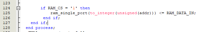
Let us now write to the ram, by setting the ram chip select (
RAM_CS) high. The address signal was set earlier and the data is the
RAM_DATA_IN input.
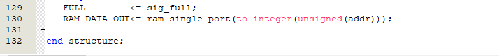
Finally, the
sig_full signal is assigned to the
FULL output. We need to know when the ram is full but not when it is empty. The
RAM_DATAOUT is output enable always and the address is also the
addr signal.
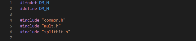
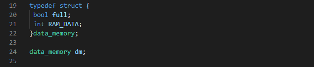
5.5 datamemory.h
The databus unit provides the ram address and ram data. Remember it has two outputs, and depending on the type of instruction one of the outputs will serve as the ram address while the other will be the ram data. Therefore, we would include the ‘mult.h’ header file which is the databus header file. The databus is also referred to as multiplexer unit. We also include the ‘common.h’ . The brainIO has a 16-bit data size, and during a register indirect addressing, the 8-bit ram address is stored in the register. So we would need a new function that would extract bits 7 down to 0, from the 16-bit register. We call this function ‘splitbit()’. Therefore, I have included ‘splitbit.h’ to use this function.
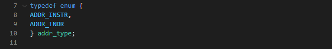
The ram address can either be part of the instruction(direct addressing) or stored in a register (register indirect addressing). So we create an enum called
addr_type to store this operation.
ADDR_INSTR- for address in instruction and
ADDR_INDR- for address stored in register.
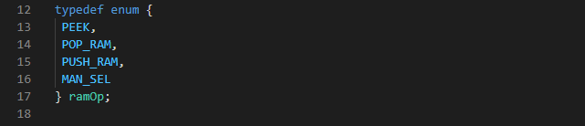
Next, lets create another enum to store the : peek, pop, push and manual select operations. This enum is called
ramOp.
Next, we create the data memory struct called
data_memory dm. This will store the data memory output:
RAM_DATA(output of the ram) and
full(ram full).
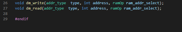
Lastly, we would declare two functions for the ram read and write. These two functions would have three arguments.
1.
addr_type: whether it is direct or indirect addressing.
2.
address: stores the actual address for a direct addressing. For an indirect addressing it is either left as null or zero.
3.
ramOp: For direct addressing, it is always
peek.
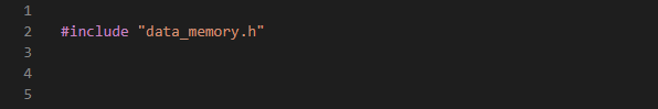
5.6 datamemory.c
We include the ‘datamemory.h’ header file.
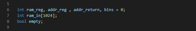
Next we would declare some variables we would use. The
ram_in array is our ram. The rest would be discussed later.
The data to be written to the ram is stored in the data bus output called
MULTOUT which belongs to the struct called
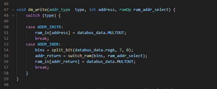
databus_data . As for the address, different ram addressing needs different method of read or write. So, for the write operation we would first switch the
type. If It is a direct addressing, we would store the data to the address contained in the instruction, that is the address in the argument. If it is a ‘register indirect addressing’ then the address is in the databus second output called
regA which is also part of the
databus_data struct. Since this databus data is 16-bit and the ram address is 8-bit, we would use the splitbit() function to extract bits 7 down to 0 of the databus output. The splitbit() function takes three arguments: the main data to extract from, the starting bit and the stop bit. After extracting the address, we need another function to know which address format to use , whether it is : pop, push, peek or man_sel. This function is called ‘switch_ram()’. It takes two argument, the
address and the
ram_addr_select. The ram_addr_select contains the actual select option.
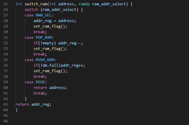
The switch_ram() function switches between the different ram operations. For a
man_sel -The address register stores the new address. For a
push or
pop - The address register increments and decrements respectively. For a
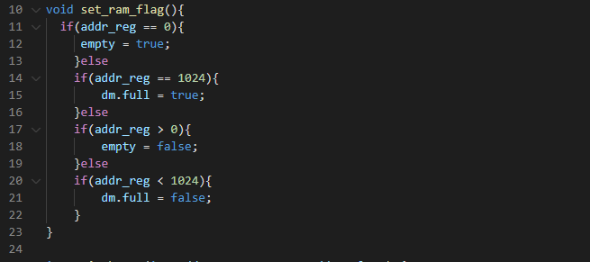
PEEK- The address is returned without being stored. For each operation the ‘set_ram_flag()’ function is called to determine the state of the ram. This function determines if the ram is full after a push operation or empty after a pop operation.
After each operation, the ‘set_ram_flag()’ function checks if the size of the ram array is 0 or 1024. If it is 0, then it sets
empty high and this prevents a further pop operation in the ‘switch_ram()’ function. If it is full it sets
full high and prevents a further push operation. We need to know when the ram is full not when it is empty, so we store the
full in the data memory struct called
dm. This will make it accessible outside the data memory unit.
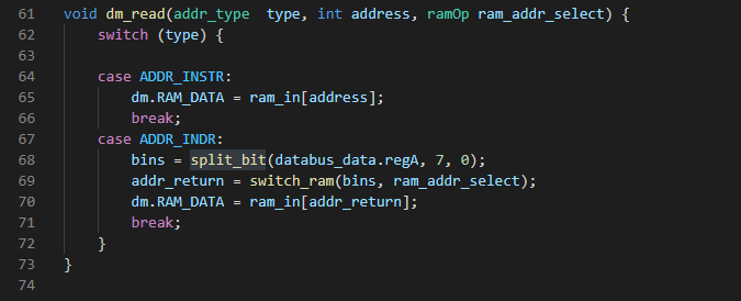
Lets define the read operation. The read operation is almost same with the write operation except that here there is data to be written rather data is read. We would also switch the address type and for a direct addressing we would use the
address in the instruction and store the output in the data memory output called
RAM_DATA which is stored in the data memory struct called
dm. For indirect addressing we would use the
bins variable to extract bits down to 0 from the data bus output called
regA, contained in the databus struct. The generated address is passed to the switch ram function and the returned address is used to access the ram. The output is stored in the
RAM_DATA.