Why this? Why not artificial intelligence or robotics or machine learning etc.? Computer architecture is versatile and is at the bedrock of all old and modern day sophisticated technology. The chips used to build the robots, the virtual reality goggles used in the METAVERSE, the artificial intelligence satellite tracker which runs on a microcontroller, the bitcoin hardware cold storage, NFT upcoming technology, Samsung latest flip phones etc. all these mind blowing technologies have computer architecture at its frame work and It has continued to open new gate ways to modern inventions.
Why an SOC? In a layman’s understanding, a unique difference between an SOC and other circuits maybe an SPI, UART, MODEM etc. is that an SOC runs renewable instructions. A modem hardware designs performs a specific function and to perform a different task from its original design the hardware needs to be changed. SOC are hardware built to run other programs stored in the memory, and by changing the data in its memory it can perform other functions without changing its hardware. So I decided to design an SOC because I want to run renewable codes just like an Arduino or raspberry Pi.
What type of interface will they have? I also wanted some kind of output. I have studied and worked with a lot of SOC design which usually served as an interface or a brainbox for a bigger design. Some were used for image processing, video processing, attached to a wishbone interface, Axis interface, or left with an interface that allows anyone further develop it. I decided to add i/o ports so they can be interfaced directly to a sensor or an LED or used to control other more complex designs.
What is the target device? Here, two options were available. Implementing the design on a microcontroller which required a high level understanding of the C language or implementing the design on an FPGA which required knowledge of an HDL language. Since the project was for educational purposes I decided to implement on both languages. The codes were originally written in VHDL and later translated to the C language. This is to enable users of both languages eligible for the course. One major characteristic of this design is bit manipulation. Shifting bits, merging bits, splitting bits etc. these operations were easier in VHDL but separate function blocks were used in C to overcome this challenge.
What is the size of the machine? This can range from 8-bits, 16-bits, 32-bits, 64-bits or more. From experience, designing mini circuits like a BPSK modem or an i2c circuit or some circuits used for classroom lectures can compatible with an 8-bit data size. Circuits that handle large data example is an OFDM circuit, Ethernet-TCP/IP protocol model, circuits used in data encryption like RSA, AES, SHA-256 etc. all require large data sizes at least 32-bits or more. SOC are highly integrated models and require large data sizes too, for this course the least possible was a 16-bit data size.
What subsystems are needed? An SOC is highly integrated, at its core is the CPU which must at least have an ALU and some registers. It integrates a lot of electronics and computer system such as memory (ram or rom), i/o port, stack, timers etc. In this course I have referred to them as units, sub systems or sub units. The need for these other units depends on the designer and what he wants to achieve. I included ten sub units which I will give reason why I added them while discussing each of them in later chapters.
Lastly, what computer architecture, model or instruction set will the machine use? RISC (Reduced Instruction Set Computer), CISC (Complex Instruction Set Computer), MIPS, hybrid, control/datapath model, Harvard architecture, Von Neumann architecture etc. These are some of the designs I have come across. Conventional high level languages where codes are processed serially (one line after another) were modelled using RISC machine. RISC runs fewer instructions per clock cycle compared to a CISC machine which runs complex instructions in parallel. During the design, it was easier to picture the codes running on BrainIO because it was designed with RISC. Hybrid machine combines features from both. MIPS is a modular architecture and processes data stage by stage. it uses Fetch -> Decode -> Execute -> Load -> Store to process batch data. The control/datapath model mostly do not incorporate a ram, it has a separate data unit and another unit called control which processes data. Von Neumann architecture incorporates a ROM which I didn’t see any need for it in this particular design. So, I chose the Harvard architecture because they are more suited for CPU models compared to others listed above.
Finally, what is the name? ’BrainIO’. Lol
1.1 BRAINIO is a 16-bit miniature microcontroller based on the RISC instruction set and Harvard architecture. It can read data input and give output signals using its extensive arrays of bi-directional i/o ports, interrupt pins and PWM pin. The chip can be controlled using a high level language which I would develop 'WALKALONG: 2' or a simplified embedded c program. The core consists of twenty-eight simplified instruction set, which can be improved up to 40 instructions or more. With 7 general purpose registers which are directly connected to the Arithmetic Logic Unit (ALU), this allows two independent registers to be accessed in one single instruction executed in one clock cycle. Each of the registers are also independently accessed by one of the different sub units and controlled using either the push or the chip select signals e.g. fifo, timer, ioport, lifo, ram etc.
1.2 Features
– Harvard Architecture
– 28 Single-clock Cycle RISC Instructions
– 16-bit up/down Timer/Counters
– 5 16-bit General Purpose Working Registers
– UART Interface
– 3 external interrupt pins
– 1 PWM pin
– 4 x 8 Bi-directional I/O Lines
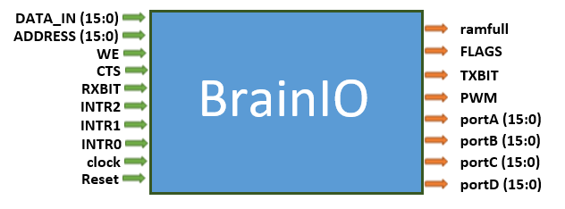
Typical pinouts contained in this course are based on simulations. The address, Data_in and we
(write enable) are used to load the software program on to the instruction memory. When the we (write_enable) pin is enabled, program or instruction is being load into the core and this prevents any instruction from running. The address signal contains the address in memory where each instruction is to be stored while the data_in contains the actual instruction.
The rxbit (received bit), CTS (clear to send) and txbit (serially transmitted bit) are used
for the UART(Universal Asynchronous Receiver and Transmitter) data transmission and reception. Other UART pins includes the RTS
(Ready to send), error (checks for error during data transmission or reception) and txdone
(signals the end of a successful transmission). In a future version of BrainIO, the UART will be used to load the program instruction. Here, it is used to load a seperate FIFO unit which we would discuss later.
Three external interrupt pins are available: NTR0 , INTR1, INTR2. Their order of priority increases from INTR2 down to INTR0. Their mode of operation would be discussed extensively while we discuss the program counter register.
One PWM(Pulse width modulation) pin (PWM) which produces a steady fixed frequency. These pins can be configured using a software program.
A single clock line and a single reset line are both used to synchronize the whole chip. ALU flags like carry flag,
zero flag, negative flag is represented using the flag line. The ram_full
signals when the data memory is full. This ram stores all variables contained in the software program.
four 8-bit bi-directional I/O port, labelled portA , portB , portC and portD
can be configured as input or output. Each of the pins of the ports can be addressed independently and can have a different port direction from other pins in the same port.
1.4 SUBUNITS
The core has the ability to access memories, perform calculations, control peripherals, and handle interrupts with separate memories and a common bus for program and data. Instructions in the program memory are executed with a single level pipelining. While one instruction is being executed, the next instruction is pre-fetched from the program memory. This concept enables instructions to be executed in every clock cycle. All memory operations including memory read or write is completed in a single clock cycle. The BrainIO architecture consists of ten sub systems on which I would section this course . They include:
- Alu
-Data Memory
-Instruction Memory
-Decode unit
-Registers
-LIFO (last-in-first-out) or Stack memory
-Timer unit
-IOPORT
-Data Bus
- UART / FIFO unit