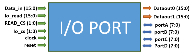
data_in which is used for a write operation and the IO_READ which is used for a read operation. This aims to optimize this unit making it possible
to read and write to the i/o port at the same time without interruptions. The io_cs signals enables the chip select for this unit.
It also controls whether to write to the port data register or the port direction register. The READ_CS signal is used during a read operation to determine which port to read and in what order to read them. The ports :portA, portB , portC, portD
pins are bi-directional and can be configured as input or output depending on the port direction register. This have two data ouputs called dataot1 and dataout2.Example: write ‘1011’ to portC[5:2]
1st clock cycle: The io_cs signal would be set to ‘11’ to write to port direction register
The io_data signal bits 15 downto 8 would be set to ‘00111100’
The parts marked one represents bits 5 downto 2, and the bit ‘1’ sets it as output
2nd clock cycle: The io_cs signal would be set to ‘01’ to write to port data register
The io_data signal bits 1 downto 0 would be set to ‘10’
The value ‘10’ selects port C. (00-selects portA, 01-selects portB, 11-selects portD).
A constant 0xFF is used to select the pins 5 down to 2
The io_data signal bits 2 downto 0 would be set to ‘010’
The io_data signal bits 5 downto 3 would be set to ‘101’
The constant 0xFF is shifted to the right by ‘101’ and to the left by ‘010’
The result is : ‘00111100’ = pin selector. This aligns exactly at bits 5 downto 2
The io_data signal bits 13 downto 6 would be set to ‘00001011’
The data to be written which is ‘1011’, is written from the left most bit
‘101’ - ‘010’ = ‘011’; substract the max from the min
Shift bit 13 down to 6 by 3 : ‘00001011’ << ‘011’
The result : ‘00101100’ = data
The selector is used as a multiplexer to select only the desired bits which is 5 downto 2
Only the selected bits would be filled with their respective data which is ‘1011’ and no longer
‘00101100’
All these steps are completed in only two clock cycles. One cycle to set the pin direction and another cycle to write the data. The pin or port direction is set only once,
therefore this step would take only one clock cycle on another operation.
READ_CS is used to determine the nature of the two data outputs. | READ_CS | Data_out0 | Data_out1 |
|---|---|---|
| 00 | PORT0 | PORT0 |
| 01 | PORT0 | PORT1 |
| 10 | PORT1 | PORT0 |
| 11 | PORT1 | PORT1 |
Example:
given portA=>'11000101', portB=> '00101011', portC=>'10110111', portD=> '10000101'.
Therefore, PORT0 => '1100010100101011'=> portA & portB.
PORT1 => '1011011110000101' => portC & portD.
Read port0[13:5] and port1[7:0] ?
The READ_CS needs to be set to '01'.
IO_READ bit 7 downto 0 is used to control data_out0 while bit 15 downto 8 is used to control data_out1.
To read port0[13:5] into data_out0: a0 = 15-13 = 2; b0 = 5 + 2 = 7.
To read port1[7:0] into data_out1: a1 = 15-7 = 8; b0 = 0 + 8 = 8.
a0 = 2, b0 = 7, a1 = 8, b1 = 8.
Therefore,IO_READ = '2,7,8,8' = '1000 1000 0111 0010' and READ_CS = '01'We need to shift PORT0 to the left by IO_READ[3:0] and then to the right by IO_READ[7:4] => '0000 0000 0010 1001'
We need to shift PORT1 to the left by IO_READ[11:8] and then to the right by IO_READ[15:12] => '0000 0000 1000 0101'
The major reason the dataout values and the final data_in values are not aligned at the exact position, rather they are padded with zeros from the left. (e.g port0[13:5] which is ‘00 0101 001’ is written as ‘0000 0000 0010 1001’ instead of ‘0000 0000 0101 0010 0000’) is because aligning the bits introduces error at the ALU during computation.
Example if I want to add two group of bits say portC[7:4] = ‘1011’ and portA[3:1] = ‘011’ at the ALU .
Adding aligned values:
10110000 + 00000110 = 10110110 = 182 in decimal (error)
Adding right aligned bits
00001011 + 00000011 = 1110 = 14 in decimal (correct)
So, aligning the bits to the left is more accurate than aligning them at their significant bits


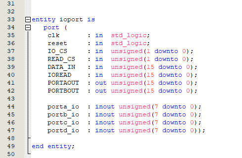
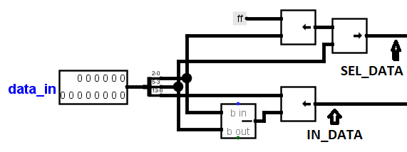
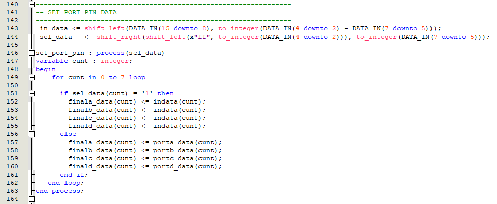
IO_CS which is the IO port chip select has two bits. Bit0 is used to set the IO port for a write operation, while bit1 when high selects the port direction for the write operation and when low selects the port data for a write operation. Bit 1 downto 0 of the IO port data_in is used to select which port direction or port register to write to. There four port data registers and four port direction registers. The port direction register takes as input bit15 downto bit8 of the port data_in as its input while bit 7 downto 0 are used as control signals.
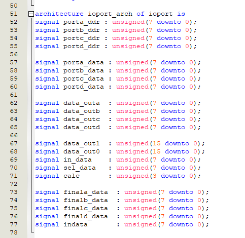
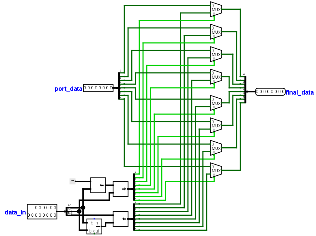
DATA_IN but are converted with the algorithm explained above. The port data registers: porta_data, portb_data, portc_data, portd_data takes as input finala_data, finalb_data, finalc_data, finald_data. We would derive these signals next. 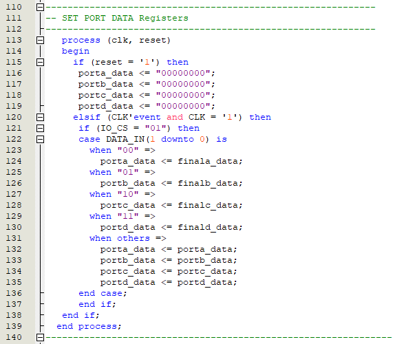
DATA_IN to the left and to the right. 
data_outa, data_outb, data_outc, data_outd are the main data outputs from each port. We will also address each pin independently using a for loop. The loop will check if the pin is an output or input and it will select the data output based on this. 
dataout0 and dataout1. The READ_CS will select this output. Finally we use the read algorithm explained above to generate the outputs.
iodata io_data.This struct will consist of all the IO unit outputs. The output includes two data outputs and four 8-bit IO pins. 
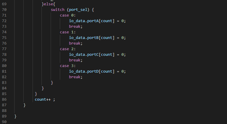
io_write()- Used to write to the port direction register or the port data register. port_read() - Used to read a single pin or a group of pins. port_write() - used to write to port. data_write - writes data to pins. readpin - read pins. 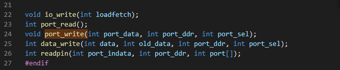
ioport.h. We would also use a lot of integer variables. 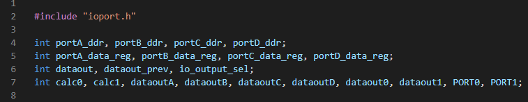
io_write() is used to set the pin direction or pin data. Its argument will be the chip select called loadfetch. Bit0 is used to turn on the IO unit and bit1 is used to switch between writing to pin data register or pin direction register. These bits are converted to decimal here. i.e ‘00’=>0, ‘01’ =>1, ‘10’=>2, ‘11’=>3. Therefore, when it is ‘11’ or 3 then the port direction register is selected. Bit 15 down to 8 of the reg_data.IO_DATA is written to the selected port direction register. Then it also calls the port_write() function. 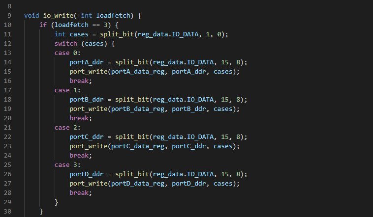
data_write() function. 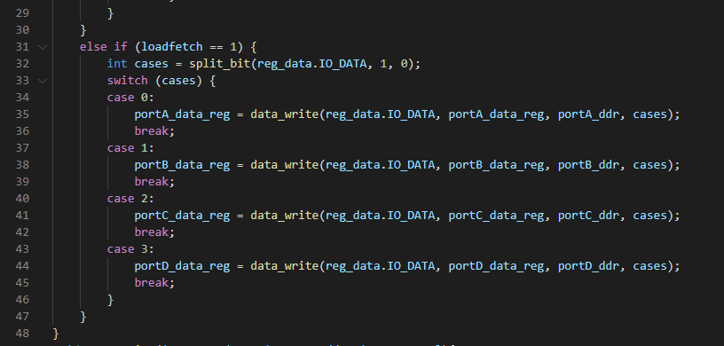
port_write() is called, it loops through all the bits of the port direction register if the bit is equal to one , that is if the bit is set to output. If it is set to output it will set its value to the value in the port data register .That is if the pin data register is equal to one it will set the pin high. 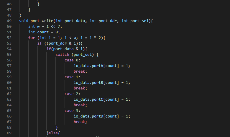
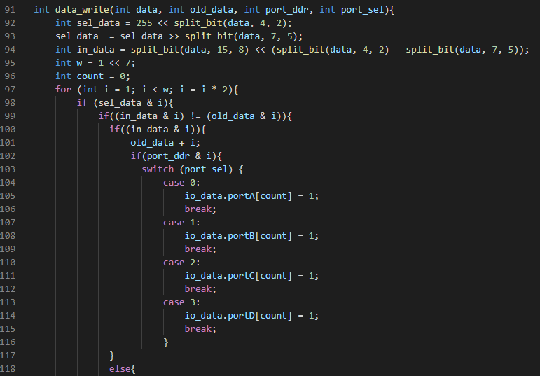
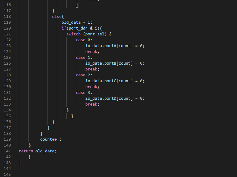
data_write(). It uses the algorithm explained earlier to convert the data input. It is also depicted in the picture below. 
splitbit() function is used to split bit , we would create a new function called concatenate() which would be used to join bits together. This function takes the two bits, converts the integers to string, then concatenate the strings, convert it back to integer and return the output. 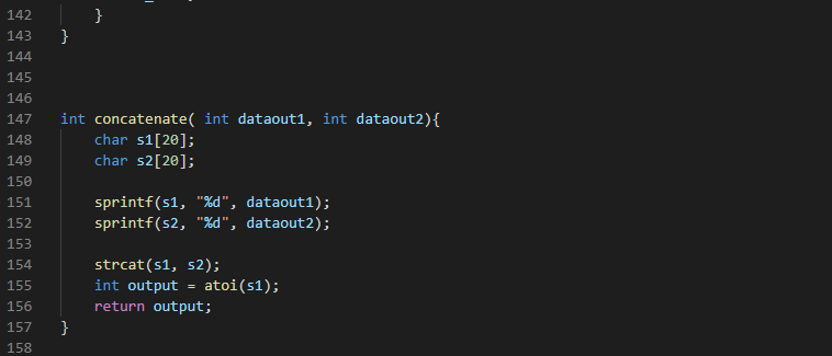
readbit(). This function loops through the pins in each port and reads their values. It will first check if it is set as an output, then it would read its pin data register else if it is set as an input it will read its pin. 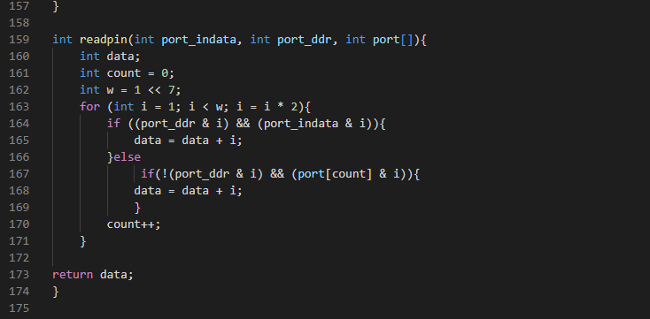
readpin() and concatenate() function, let us write the port_read() function. At the output, portA and portB are concatenated to form a single 16-bit register while portC and portD are concatenated to also form a 16-bit register , this is because that is the size of our databus. Our IO port have two main data outputs which is defined by the READ_CS signal. This signal determines which group of output ports to read , whether (portA and portB) or (portC and portD). The READ_CS is two bit. A ‘0’ selects (portA and portB) while a ‘1’ selects (portC and portD). Which one comes first depends on the position of the zero or one. Note, they are in decimal values here.
