6.1 Why do we need a Cache?
Every student of computer science knows what a cache is, A temporary storage.It is used between the processor and memory since they both have different speed. So, what other type of design would require it? Most SOC and CPU chips i came across were designed to decode instructions that came through an external interface. That is, they do not have a seperate program memory were instructions are stored. For these designs the external instructions dictate the rate at which is processed in the CPU. For other models like BrainIO which have its own program memory, If its I/O ports were to serve as an interface to receive data or instruction from an external circuitary whose rate of transmitting information is higher than the rate at which the CPU processes this information. Then, there is a need to store this information so that the processor can process them later when its free. Another instance that requires a cache. If the program memory instruction is not dedicated to processing the information that comes through the external interface or I/O port(that is, if it has other functions its performing which will result to its unavailability to process data coming through the interface) and if the I/O port constantly receives data, Then we would need to store the information and then request them only when the instruction requires them. In summary, any design that might result to data loss due to unavailability of the CPU or the unit that needs to process the data would have to optimize the design or incorporate a cache which would store the information and make them available only when needed.
6.2 The Fifo
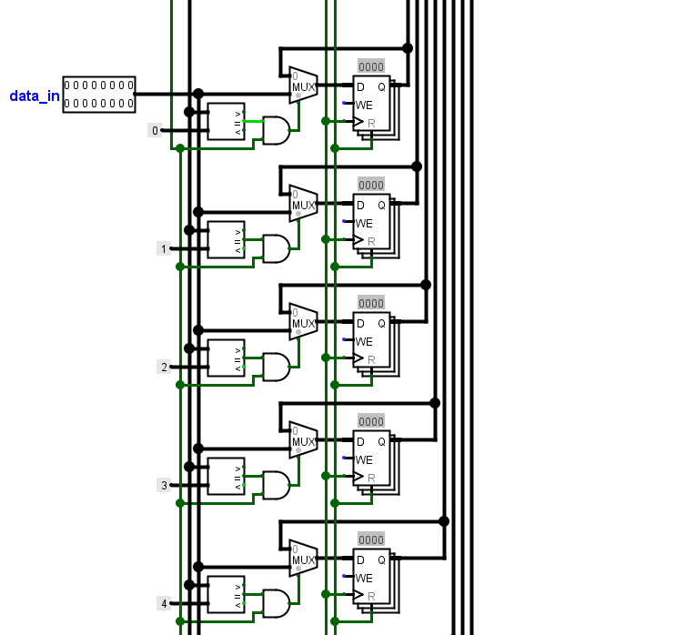
BrainIO implements the fifo cache. It consists of eight 16-bit register used to store data with two 3-bit address register for the push and pop operation. FIFO stands for First-in-First-out. The first data to stored into this cache is the first data to be output. The FIFO has two main operations. The push operation used to push data on the cache and the pop operation used to output data from the cache. The CPU push excess data on to the cache when its busy and pops them whenever it wants to process them. in this way, no data is lost. Each of these operations has its own 3-bit address register which counts from '000' to '111' and stores the address of the next register to pop or push. Initially, when the FIFO is empty both address registers are equal to zero and the empty signal is turned on. This signal prevents a further pop operation and allows only a push operation. When a push operation occurs its register increments and is now gretaer than the pop register. when a pop operation occurs its register increments and becomes equal to the push register and the empty signal comes on again. Therefore, the empty signal is designed to turn on whenever the pop register euals the push register and at this point, no further pop operation is allowed. Futhermore, whenever the push register increments upto b'111' its register starts from zero. At this point if a further push operation keeps occuring and the push registers increments upto one register below the pop register, then the FIFO is assumed to be full. example, if pop register is at 5, and the push register has increased upto 7 and starts afresh from zero. If it gets upto 4, then the unit is full. This is because data in register 5, 6 and 7 are yet to be popped, therefore pushing data on to them will overwrite the previous data. The full signal turns on when the push register is equal to the pop register plus one, at this point no further pop operation is allowed. The two 'AND' gate are used to ensure this two conditions are met before a push or pop operation occurs.
The eight storage regsters are depicted in the schematic above. For data in the DATA_IN to be pushed onto one of the register, the push signal must be turned on and the push register must contain the address of that particular register. A comparator is used to compare the push register address and the address of the register. Consequently, the FIFO_OUT must contain the register data whose address is in the pop register. In a layman's understanding, the push operation fills a register increments its address to be able to move to the next register while the pop operation reads data which was filled by a push operation, then increments its address to go to the next register to read another data pushed by a push operation and this cycle continues.
6.3 The PINOUT
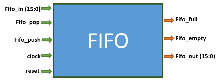
The pins consists of the FIFO_in which contains the data to be pushed. fifo_pop and fifo_push which is used to signal a pop or push operation. fifo_out, this is the output of the fifo. full and empty, they signal the state of the fifo.
6.4 FIFO.vhd
First we declare the title.
Next we declare the IEEE; standard library
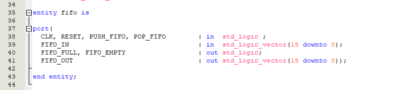
Next is the port. These are the pinouts we discussed in earlier section.
The signals Consist of eight 16-bit register block labelled reg0 down to reg7 with two address registers labelled regA and regB.
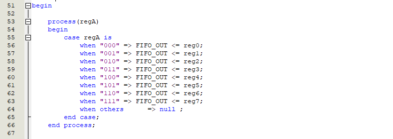
Let us use regA as the address for a pop operation. It will serve as a pointer to the address of the register we want to pop to the FIFO_OUT.
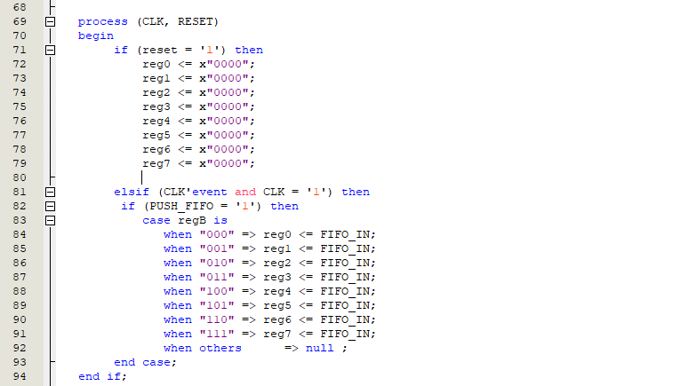
Let us use regB as the address for a push operation. It will serve as a pointer to the address of the register we want to push the FIFO_IN data. The code for the pop and push are different because for the pop operation above, the outputs of the registers are directly connected to the FIFO_OUT through a multiplexer, while for the push operation, the registers are behind a clock.
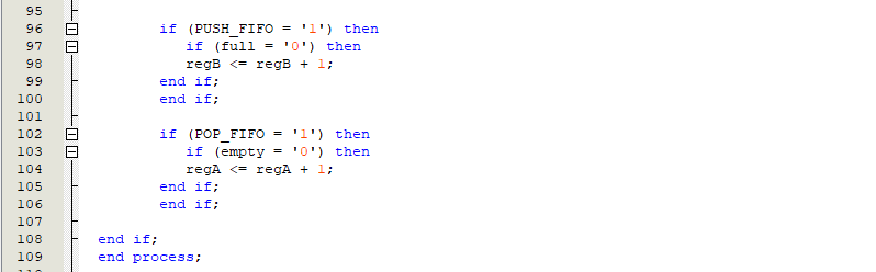
The full signal is used to make sure that regA is not equal to regB + 1 before incrementing it for a push operation while the empty signal is used to make sure that regA is not equal to regB before incrementing during a pop operation.
Initially, when the fifo unit is empty. Both register A and register B are zero, and this turns the empty signal On. Whenever there is a push operation regB increases, and during a pop operation, regA increases. Whenever both registers become equal, this means the fifo unit is empty. consequently, whenever the push register fills up to "111" it returns to zero, and when it is one step behind the pop register, then the fifo register is assumed to be filled up.
The full and empty signal will be assigned to the FIFO_FULL and FIFO_EMPTY respectively.
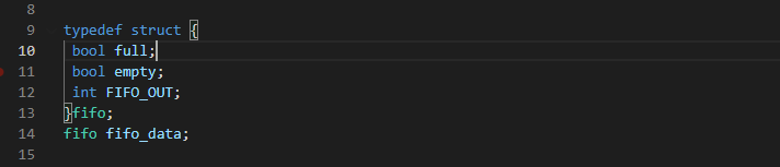
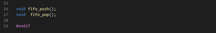
6.5 FIFO.h
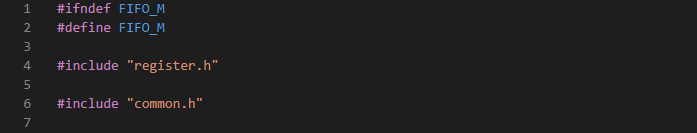
The register unit consists of a lot of registers that send data to other units including the fifo, lifo, timer etc. Data to the fifo unit comes from the register unit so we will start by including the register header file to access it. Also the common.h to enable standard libraries.
Lets create the fifo struct which will contain the outputs of the fifo. We also need to read when the fifo is full or empty, this will be read by the register unit. We would check if the fifo is full or empty and if so, we can adjust the program counter to skip to certain instruction.
The fifo unit will have only two operations push and pop. We would now declare this two functions here.
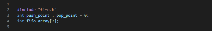
6.6 FIFO.c
We would start by including the fifo header file. The fifo_array will serve as the array of registers used for storage in the fifo. The push_point represents the push register or register B while the pop_point represents the pop register or register A.
Let us now write the push function. We will first of all check if the fifo is full, which is when register A is equal to register B +1. If it is full, we will set the full signal in the fifo struct called fifo_data to be true and exit. If it is not empty, then we will proceed to write the FIFO_DATA which is in the register struct called reg_data to the array of fifo registers using the push_point or register B as the address. Finally, we increment the push point.
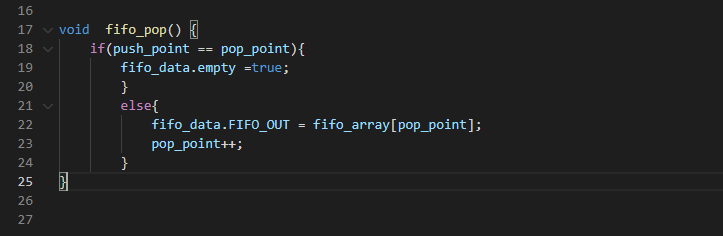
Let us write the pop function. We will first of all check is the fifo unit is empty before we pop. This is when the push_point equals the pop_point. If it is empty, we will set the empty signal in the fifo struct called fifo_data to be true and exit. If it is not empty, then we will set the FIFO_OUT which also part of the fifo struct to the data in the fifo registers using the pop_poin as the address. Then finally we will increment the pop_point.
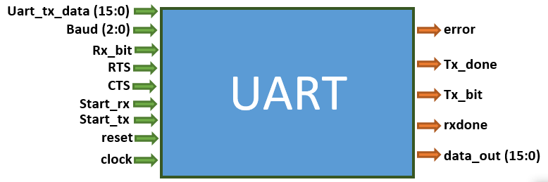
6.7 The UART fifo Cache
The brainio is a typical example of a CPU which is not dedicated to any of its interfaces. It runs its own instruction in the program memory.
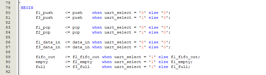
We would demonstrate the use of the cache by adding an UART to the fifo interface. Instead of the cache unit consisting of a single fifo, it would consist of three fifo units and one UART.Here, the UART will have two fifo units; one would be used to store its received data and the other would be used to store the data it would transmit. The last fifo would be a standalone fifo we can use in a case we want to disconnect the UART. The schematic is given below . The UART select bit would be used to switch between the standalone fifo and the uart with its two fifo units.
This UART, is a seperate tutorial which i already taught. It can be found at https://projectfpga.com/uart/. I would treat it as an IP block here. refer to the original course for more information.
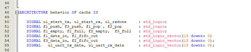
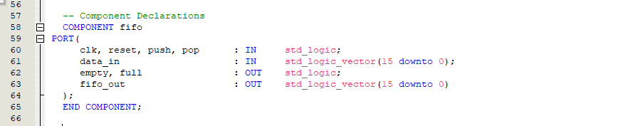
6.8 cache.vhd
First we declare the title.
Next we declare the IEEE; standard library
Next is the port. These are the pinouts we discussed in earlier section.
The signals which will be used for connecting the fifos and the uart.
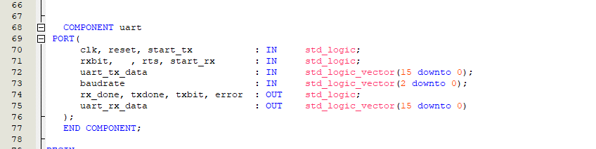
Let us introduce the FIFO component
We will also introduce the UART component
The UART which selects between the single fifo and the uart with its two fifo. Line 89 , 90 , 91.
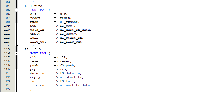
port map for the single fifo
port map for the two uart fifo
The UART port map
You can aswell ignore the uart block and treat the Cache as a single fifo unit.