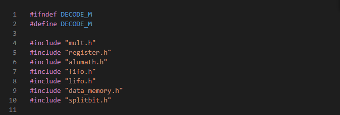
regAsel(9 downto 6) and mult_sel(5 downto 2). The opcode is also set using bit 13 downto 10. In a case, the registers can also be fed by popping the fifo or lifo, therefore the bit0 or bit1 is also set.

push_lifo on bit7, push_fifo on bit6, io_cs on bit 5 downto 4, timer_cs on bit 3 downto 2, pop_lifo on bit1 and pop_fifo on bit0.jmp_pc_ctrl, this signal is used to set the condition for a jump example jump when the fifo is empty or an alu operation is equal to zero etc. bit 7 downto 0 is used to set the jmp_pc_data, this is used to indicate how many steps to jump up or down.


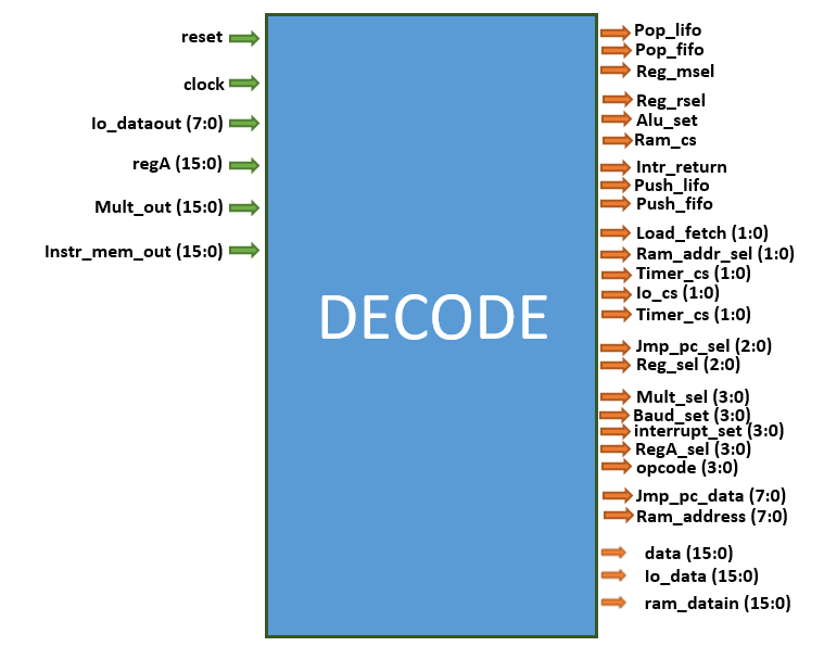
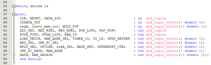
clock, reset used to synchronize the unit. instr_mem_out ,
this is the actual instruction that comes directly from the program memory. Two data inputs: mult_out and regA ,
these are the two major outputs from the databus, here parts of them would be used for memory indirect addressing. The io_dataout signal,
is the actual data output from the i/o port. The i/o port has an 8-bit output on a 16-bit machine, so here the 8-bit output will be converted to a 16-bit data output
called the io_data .
At the output of the decode unit: pop_lifo, pop_fifo, push_lifo, push_fifo these signals control the LIFO and FIFO unit.
PUSH to input data, while POP is used to remove output. timer_cs, io_cs, load_fetch, ram_cs , these three signals are used as chip select for other sub units.
They are 2-bits of data attached to every "register write" instruction. When data are sent to the registers,
their values determine if the data is also copied to their unit or stored only to the register.
Example, you can store data on the timer and fifo register , then carry out a logical or arithmetic operation on them and store in the memory OR you can store the data in the
timer register and then copy it to the timer unit. So, the chip select determines if the registers are serving as a general purpose register for ALU operation or as a data storage
for their sub unit. The alu_set signal informs the alu register to store data after an execute operation while the opcode
determines the alu operation to execute. During a "register write " operation, the reg_msel signals indicates that the data is coming from the memory while the
reg_rsel signal, indicates the data to be stored is coming from another register. These two signal are very crucial during a "register write" operation ,
this is because data from memory and register arrive at different time. Data from the memory lags a clock cycle from data from the register.
reg_sel signals stores the address of the register where data is to be written. When the CPU receives an interrupt,
it skips the current instruction and jumps to the interrupt instruction. After executing the instruction,
the intr_return signals it to return back to the current instruction it was executing before the interrupt.
Setting the ram_addr_sel signal will make the ram act like a stack , rather than access the ram with an address,
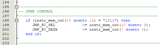
it will be accessed using a pop or push instruction depending on the value of this signal. The jmp_pc_data, jump_pc_sel is used to jump to a particular instruction,
this is useful when working with functions where particular code block needs to be executed rather progressing down the memory serially.
mult_sel, regA_sel signals are used as select signal for the data bus. baud_set signal is used to set the UART baud rate and also to turn it on/off ,
it also sets the cache_set signal in the register unit , which switches between FIFO and UART.
The interrupt_set signal, is used to set options for the interrupt. It is well described in the register unit.
The ram_address, ram_datain signals are used to set the ram. The ram_datain signal sets the data for a write operation to the ram,
while the ram_address is used for both a read or write operation.
pop signal. This signal is triggered whenever an instruction with a pop is being executed. 
pop signal is triggered, the decoder sets the PUSH_LIFO and PUSH_FIFO signals to bit0 and bit1 which are the pop bits. The value of these signals determines if the pop would be triggered. When they are low, no pop operation is triggered except either bit is high. During an alu execution, the address of the registers are explicitly defined even when they are the LIFO or FIFO registers. Therefore, during a pop operation except if it is an ALU instruction, if the lifo is popped then the databus address is set to the address of the lifo register which is ‘1010’ else it checks if the fifo is popped and sets the databus to its address. 
DATA_SIG signal whenever it receives a data instruction. This signals is used to latch the data instruction in the data register. 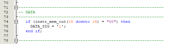
MULT_SEL holds the address of registerA, while regAsel holds the address of register. These two multiplexer selectors have their outputs on the MULT_OUT and regA respectively. The OPCODE selects the alu operation to be performed. The operation will only pop the selected registers without changing the databus outputs. Finally, the alu_set signal is used to store the output of the ALU operation. 
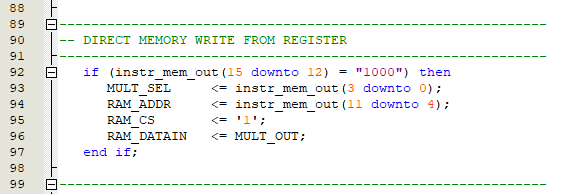
All memory write operations are from registers.
RAM_CS (ram chip select) is set to ‘1’ and the ram_datain is set to the databus MULT_OUT during a memory write operation. The MULT_sel will set the data and the ram_address are directly contained in the instruction.
regAsel signal. The selected register bit 7 downto 0, will be the ram address. For an indirect addressing the ram_addr_sel is used to switch the ram address using POP, PUSH, PEEK, MAN_SEL. The RAM_CS (ram chip select) is set to ‘1’ and the ram_datain is set to the databus MULT_OUT during a memory write operation. 

regAsel signal. The selected register bit 7 downto 0, will be the ram address. For an indirect addressing the ram_addr_sel is used to switch the ram address using POP, PUSH, PEEK, MAN_SEL. The RAM_CS (ram chip select) is set to ‘1’ and the ram_datain is set to the databus MULT_OUT during a memory write operation. The MULT_SEL signal will hold either the address of the fifo or lifo register as determined by the pop instruction. 
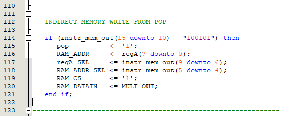
RAM_CS (ram chip select) is set to ‘1’ and the ram_datain is set to the databus MULT_OUT during a memory write operation. The MULT_SEL signal will hold either the address of the fifo or lifo register as determined by the pop instruction. 

For register write operation, data can be written from register or memory.The register data inputs are directly fixed to the MULT_OUT and RAM_DATAOUT no signal is required to select this.
REG_MSEL is set to one. The REG_SEL contains the address of the register to be written to. The LOADFETCH contains the register chip select. When it is set to zero the data is only stored in the register and would not be triggered in the sub unit. 

regAsel. Bit 7 downto 0 of regA contains this address. For an indirect addressing the ram_addr_sel is used to switch the ram address using POP, PUSH, PEEK, MAN_SEL. Since the data is written from memory the REG_MSEL is set to one. The REG_SEL contains the address of the register to be written to. The LOADFETCH contains the register chip select. When it is set to zero the data is only stored in the register and would not be triggered in the sub unit. 

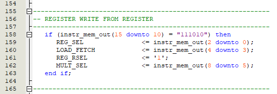
REG_RSEL is set to one indicating that data is written from a register. The MULT_SEL is also part of the instruction and contains the register or data output to be written from. The REG_SEL contains the address of the register to be written to. The LOADFETCH contains the register chip select. When it is set to zero the data is only stored in the register and would not be triggered in the sub unit. 
REG_RSEL is set to one indicating that data is written from a register. The MULT_SEL is not used here, when the pop is triggered it also sets the MULT_OUT to either the lifo or fifo register. The REG_SEL contains the address of the register to be written to. The LOADFETCH contains the register chip select. When it is set to zero the data is only stored in the register and would not be triggered in the sub unit. 


interrupt_ctrl signal. This signal is used to set most of the interrupt controls including the interrupt return register, interrupt set registers, interrupt data register and also the baud signal which sets the baud rate of the UART. 


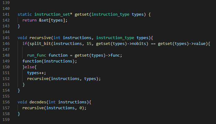
decode(). It does not have any struct to store outputs because its decoded instructions are directly executed or contained as an argument. The decode() function takes the instruction as its only argument. 
run_func() which takes the instruction as its only argument and returns void. This will enable us to treat each instruction as a function. 
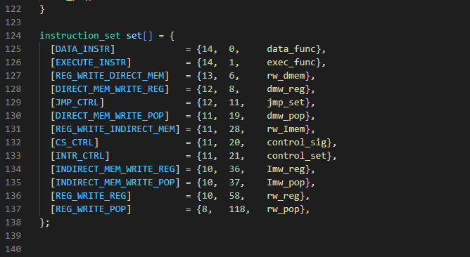
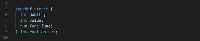
instruction_set which we will use to decode instruction. It has three items: nobits- which stores number of bits to decode, value- stores the expected value, and the run_func() which stores the function to execute.
instruction_type. This will store the type of instruction we are decoding. 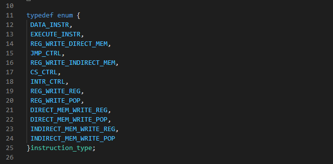
pop. Whenever a pop is triggered, the decoder checks the pop bits , if any of them is turned on then it is executed. Then it will also set the databus address to select either the fifo or lifo register. 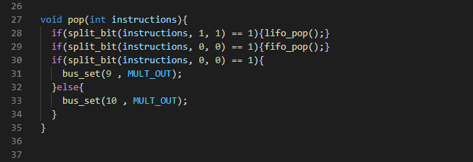
run_pc(): is used to request next instruction to decode
.1. data_func() - If the instruction is a data instruction, then the set_dataregister(). This function sets the data register to the program instruction. 
2. Exec_func() - This instruction is used for ALU operation. The two alu registers are filled by setting them to MULT_OUT and regA using the bus_set(). The opcode is set using the alu_set(). 
3. Dmw_reg() - Direct memory write from register, this is writing to the memory from register when the ram address is in the instruction as seen below. We set the MULTOUT which contains the data to be written while the address is set from the instruction. Finally, we call dm_write() to write the data to memory. 
4. Dmw_pop() - Direct memory write from the pop register. We call the pop() which pops the required register and sets the MULT_OUT. Then we set the ram address from the instruction. Finally, we call dm_write() to write the data to memory. 
5. Imw_pop() - Indirect memory write from the pop register. That is writing to the memory from the pop register using indirect addressing. regA is set to contain the register that has the ram address. We also call the pop() which pops the required register and sets the MULT_OUT. Finally, we call dm_write() to write the data to memory. 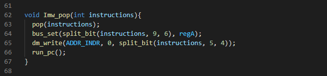
6. Imw_reg() - Indirect memory write from register, this is writing to the memory from register when the ram address is contained in a register. The instruction contains the address of the register in regA which contains the ram address. We set the MULTOUT which contains the data to be written. Finally, we call dm_write() to write the data to memory. 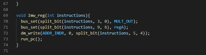
7. rw_dmem() - Register write from direct memory addressing. This is writing to a register from memory when the ram address is contained in the instruction. We would first of all, read the memory using the address in the instruction by calling dm_read(). Then we write the register using the ram output as data by setting the last argument to one. 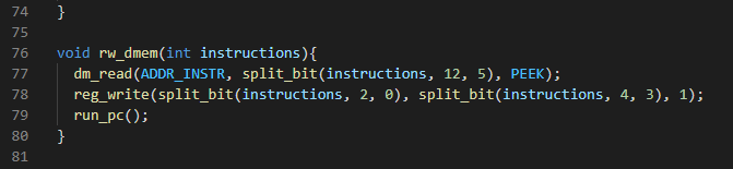
8. rw_Imem() - Register write from indirect memory addressing. This is writing to a register from memory when the ram address is contained in another register.We would first set regA to contain the register with the ram address. Then we read the memory, and finally write to the register. 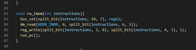
9. rw_reg() -Register write from register.This is writing to a register when the data is also in another register. Here, both the address of the origin data and the address of the destination register are both in the instruction. We simply set the MULT_OUT and call the register write. 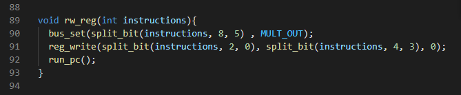
10. Rw_pop() -Register write from pop. This is writing to a register when the data is either in the FIFO or LIFO register. Here, we execute the pop() which pops either registers and sets the register to fill the MULT_OUT. 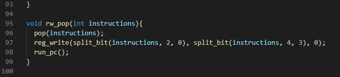
11. Jmp_set() - Jump set is used to move jump up or down the program memory. This function consists of how many steps to jump and whether it is up or down and finally the condition for the jump. 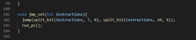
12. control_set() - This instruction is used to set the baud for a UART operation and the interrupt_ctrl signal which sets most of the interrupt operations. 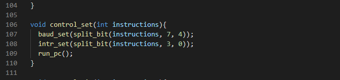
13. control_sig() - This instruction consist of chip select signals that can be triggered individually without affecting their data registers. Once the bits that are set are triggered , the rest set to zero are ignored. 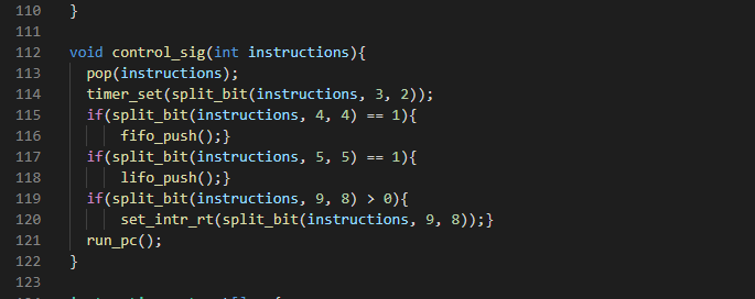
recursive(). The recursive() as the name interprets will call itself multiple times until it has matched or seen the particular instruction it is decoding. It achieves this by looping through the array below where it checks the nobits (number of bits) and compares it with the value, if it matches the current instruction it is decoding , then it will execute the run_func() attached to that instruction.