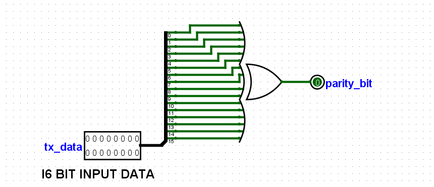
A transmitter subcircuit not included in the transmitter subcircuit is the parity bit generator. The paritybit subcircuit takes a 16-bit data from the transmitter and generates the parity bit which will be attached to the transmitter data, the receiver can check for errors in transmission using this bit. The circuit will be integrated into the transmitter using HDL (VHDL and Verilog) function, later in this chapter. The truth table can be drawn from the circuit below . The VHDL and Verilog code is also given below. The circuit is basically a 16-bit xor gate.

module parity_generator(
      input wire[15:0] tx_data,
      output reg parity_bit
  );

  always @(tx_data)
  begin
     parity_bit <= tx_data[0] ^ tx_data[1] ^ tx_data[2]
  	^ tx_data[3]^ tx_data[4] ^ tx_data[5] ^ tx_data[6] ^ tx_data[7]
  	^ tx_data[8] ^ tx_data[9] ^ tx_data[10] ^ tx_data[11]
  	^ tx_data[12] ^ tx_data[13] ^ tx_data[14] ^ tx_data[15] ;
  end
  endmodule
library IEEE;
use IEEE.std_logic_1164.all;
use IEEE.numeric_std.all;

entity parity_generator is
port(
  tx_data            : in  std_logic_vector(15 downto 0);
  parity_bit         : out std_logic);
end parity_generator;

architecture rtl of parity_generator is

begin

parity_bit <= tx_data(0) xor tx_data(1)  xor tx_data(2)
xor tx_data(3)  xor tx_data(4)  xor tx_data(5)  xor tx_data(6)
 xor tx_data(7)  xor tx_data(8)  xor tx_data(9)  xor tx_data(10)
 xor tx_data(11)  xor tx_data(12)  xor tx_data(13)  xor tx_data(14)
 xor tx_data(15) ;

end rtl;
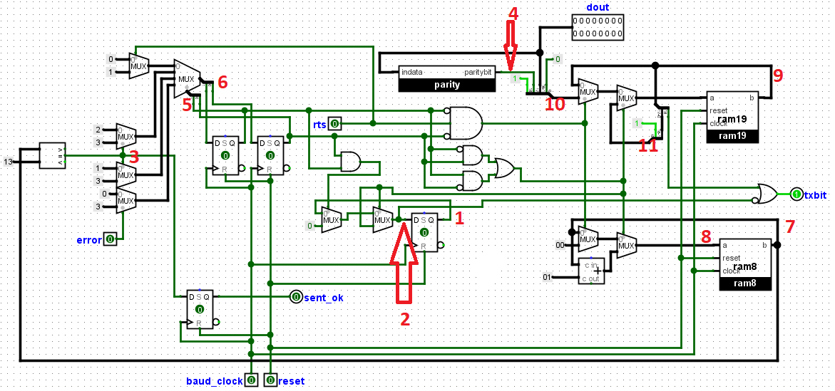
The diagram shown below is the the transmitter simulation in logism, the FSM (finite state machine) is the left side while the state action is the right side, as can be seen two flip flops are used to store the current state of the transmitter, the output labelled A and B will be fed into the state action subcircuit.You will notice that the clock driving the flip flops are not the system clock, it is the generated BAUD_CLOCK, this new clock will be fed into the transmitter through this pin as will be shown inthe last chapter.The entire circuit still share a common reset pin. The RTS pin was discussed in the architecture chapter of this tutorial, it will send the transmitter signal that the receiver is ready to receive data while the txbusy bit is set when the transmitter is currently sending data, this two bits are used to start the data transmission. The txbitcnt bit stores the number of received data, once the data is completed sent, it moves the state to the finished state. All these will be explained with the VHDL code.


This is the right side of the diagram, here we can see the paritybit subcircuit we generated earlier connected to the dataout input which is data transmitter wants to send. Also, the FSM subcircuit outputs A and B which serves as input to this subcircuit. Two Rams, ram19 which stores our 16bit data to be sent with one start, one stop bit and one parity bit making it 19 total. The next ram is ram8 which keeps counts of how many bits that has been sent out, once it counts upto 19. It stops and goes to the last state which ends the transmission. Both rams are been driven by the newly generated baud clock and not the system clock, but a common reset for the entire circuit. The txbusy bit tells the device that the transmitter is busy and it should try to transmit a new data, it turns on during transmission and off after transmission. The Area marked in Red is two wire splitters facing eachother, the upper one contains the 19bit data to be sent , then the txbit sends just one bit from it, the second lower splitter takes the remaining 18 bits and adds a '1' to it and then sends it back to the Ram. The VHDL explains it further.
--------------------------------------------------------------------------------
-- PROJECTFPGA.COM
--------------------------------------------------------------------------------
-- NAME:    UART TRANSMITTER
--------------------------------------------------------------------------------
-- AUTHORS: Ezeuko Emmanuel <ezeuko.arinze@projectfpga.com>
--------------------------------------------------------------------------------
-- WEBSITE: https://projectfpga.com/uart
--------------------------------------------------------------------------------
--------------------------------------------------------------------------------
-- UART TRANSMITTER FOR FPGA
--------------------------------------------------------------------------------
-- Copyright (C) 2020 projectfpga.com
--
-- This source file is free software: you can redistribute it and/or modify
-- it under the terms of the GNU Lesser General Public License as published by
-- the Free Software Foundation, either version 3 of the License, or
-- (at your option) any later version.
--
-- This source file is distributed in the hope that it will be useful,
-- but WITHOUT ANY WARRANTY; without even the implied warranty of
-- MERCHANTABILITY or FITNESS FOR A PARTICULAR PURPOSE.  See the
-- GNU Lesser General Public License for more details.
--
-- You should have received a copy of the GNU Lesser General Public License
-- along with this program.  If not, see <http://www.gnu.org/licenses/>.
--------------------------------------------------------------------------------

library IEEE;
use IEEE.std_logic_1164.all;
use IEEE.numeric_std.all;
use IEEE.STD_LOGIC_ARITH.ALL;
use IEEE.STD_LOGIC_UNSIGNED.ALL;
entity transmitter is
port(
  dout : in  std_logic_vector(15 downto 0); --data to be transmitted
  rts : in  std_logic;--set by receiver to tell transmitter to start sending data
  baud_clock : in  std_logic;--The baud clock, will be used instead of main clock
  reset , error: in  std_logic;
  txbit: out std_logic;
  sent_ok: out std_logic);

end entity;

architecture structure of transmitter is

signal txbusy: std_logic;
signal s_txbusy: std_logic;
signal nobits: std_logic;
signal parity_in: std_logic;
signal TXFSM : std_logic_vector(1 downto 0);
signal TXFSM_in : std_logic_vector(1 downto 0);
signal txbitcnt : std_logic_vector(7 downto 0);
signal txbitcnt_in : std_logic_vector(7 downto 0);
signal data_reg : std_logic_vector(18 downto 0);
signal data_reg_in : std_logic_vector(18 downto 0);
signal data_reg1 : std_logic_vector(18 downto 0);

--adding the parity generator circuit to the transmitter
component parity_generator is
port(
  tx_data            : in  std_logic_vector(15 downto 0);
  parity_bit         : out std_logic);--the name was changed to avoid
  --conflict with the parity_bit here.
end component;
begin
  join_parity: parity_generator
    port map (tx_data=>dout, parity_bit=>parity_in );
 -- ends here

 --adds the stopbit, paritybit, 16-bit data, and the start bit together
 --making total of 19bits to be sent out
 data_reg_in <= '1' & parity_in & dout & '0';
 data_reg1 <='1' & data_reg(data_reg'high downto 1);
 txbit      <= data_reg(18) or not s_txbusy;
nobits <= '1' when (txbitcnt = "1101") else '0';

process (reset, baud_clock)
begin
if reset='1' then
 TXFSM <=  (others => '0');
  txbitcnt <=  (others => '0');
   data_reg <=  (others => '0');
	 sent_ok <= '0';
	 txbusy <= '0';
  elsif rising_edge(baud_clock) then
 TXFSM <=  TXFSM_in;
  txbitcnt <=  txbitcnt_in;
	 sent_ok <= nobits;
	txbusy <= s_txbusy ;

	case TXFSM is

  when "00" =>
  if rts='1' then
  data_reg <= data_reg_in;
  txbitcnt <=  (others => '0');
  TXFSM <="01";
  end if;

  when "01" =>
  txbusy <='1';
  data_reg <= data_reg1;
  txbitcnt <= txbitcnt + 1;
  if(nobits = '1') then
  TXFSM <="11";
  else
  TXFSM <="10";
  end if;

  when "10" =>
  txbusy <='1';
  data_reg <= data_reg1;
  txbitcnt <= txbitcnt + 1;
  if(nobits = '1') then
  TXFSM <="11";
  else
  TXFSM <="01";
  end if;

when "11" =>
	txbusy <= '0';
	if (error = '1') then

	TXFSM <= "11";
else
   TXFSM <= "00";
end if;
	end case;

end if;
end process;
end structure;