SPI
2.0 Data transmission
To begin communication, the bus master configures the clock, using a frequency supported by the slave device,
typically up to a few MHz The master then selects the slave device with a logic level 0 on the select line.
If a waiting period is required, such as for an analog-to-digital conversion, the master must wait for at least
that period of time before issuing clock cycles. During each SPI clock cycle, a full-duplex data transmission occurs.
The master sends a bit on the MOSI line and the slave reads it, while the slave sends a bit on the MISO line and
the master reads it. This sequence is maintained even when only one-directional data transfer is intended.
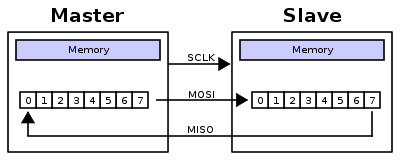
Transmissions normally involve two shift registers of some given word-size, such as eight bits, one in the master
and one in the slave; they are connected in a virtual ring topology. Data is usually shifted out with
the most significant bit first. On the clock edge, both master and slave shift out a bit and output
it on the transmission line to the counterpart. On the next clock edge, at each receiver the bit is sampled
from the transmission line and set as a new least-significant bit of the shift register.
After the register bits have been shifted out and in, the master and slave have exchanged register values.
If more data needs to be exchanged, the shift registers are reloaded and the process repeats.
Transmission may continue for any number of clock cycles. When complete, the master stops toggling the clock signal,
and typically deselects the slave. Every slave on the bus that has not been activated using
its chip select line must disregard the input clock and MOSI signals and should not drive MISO
(I.E. must have a tristate output) although some devices need external tristate buffers to implement this.
Transmissions often consist of eight-bit words. However, other word-sizes are also common, for example,
twelve-bit words for many digital-to-analog or analog-to-digital converters. Our design will consist of 16-bit data.
2.1 SPI standard
There is lack of a formal standard which is reflected in a wide variety of protocol options.
Different word sizes are common. Every device defines its own protocol, including whether
it supports commands at all. Some devices are transmit-only; others are receive-only.
Chip selects are sometimes active-high rather than active-low. Some protocols send the least significant bit first.
Some devices even have minor variances from the CPOL/CPHA modes as we will discuss later.
Sending data from slave to master may use the opposite clock edge as master to slave.
Devices often require extra clock idle time before the first clock or after the last one, or between a command and its response.
Some devices have two clocks, one to read data, and another to transmit it into the device.
Many of the read clocks run from the chip select line.
There are also hardware-level differences. Some chips combine MOSI and MISO into a single data line (SI/SO)
this is sometimes called 'three-wire' signaling (in contrast to normal 'four-wire' SPI).
Another variation of SPI removes the chip select line, managing protocol state machine entry/exit using other methods.
2.2 The SPI modes
In addition to setting the clock frequency, two very important configuration parameters
for the SPI protocol are the clock polarity
(CPOL) and the clock phase
(CPHA).
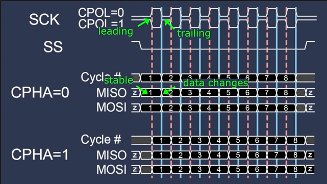
The combinations of polarity and phases are often referred to as modes. The timing diagram is shown above .
→ CPOL determines the polarity of the clock.
- CPOL=0 is a clock which idles at 0. This is demonstrated above;
the clock is initially idle at 0 and starts pulsing at 1. That is,
the leading edge is a rising edge, and the trailing edge is a falling edge.
- CPOL=1 is a clock which idles at 1. This is demonstrated above;
the clock is initially idle at 1 and starts pulsing at 0. That is,
the leading edge is a falling edge, and the trailing edge is a rising edge.
→ CPHA determines when data has to be toggled by the transmitter and when the data has to be sampled by the receiver.
- For CPHA=0, the data is sampled at the leading edge of the clock signal.
- For CPHA=1, the data is sampled at the trailing edge of the clock signal.
The SPI modes are summarized in the table below.
| MODES |
CPOL |
CPHA |
Description |
| Mode 0 |
0 |
0 |
Active state of clock is 1 and data is sampled at leading edge |
| Mode 1 |
0 |
1 |
Active state of clock is 1 and data is sampled at trailing edge |
| Mode 2 |
1 |
0 |
Active state of clock is 0 and data is sampled at leading edge |
| Mode 3 |
1 |
1 |
Active state of clock is 0 and data is sampled at trailing edge |
2.3 Pros and Cons
The SPI offers a lot of advantage over its counterparts like the UARTs and I2Cs. The slaves use Master clock and has no need
for precision oscillators or over sampler like the UART .They also do not have transceivers like UART. SPI has higher
throughput than UART since the maximum rate of data transmission is not limited to the clock speed of the devices unlike UART
where the baud rates are dependent on the clock speed of each devices. The Slaves do not use a unique address like the I2Cs
and they have higher speed in Mb/s compared to I2C and UART that are in KB/s. It has lower power consumption and reduces cable
sizes since all bus are shared except the chip select which is at most one single bus per device and also offers full duplex communication
with full protocol flexibility as to the size of bits transferred it can take any number of data bits.
Some of the cons includes that SPI configuration like the three wire bus is half duplex Requires more pins on IC packages than I²C,
even in the three-wire variant. It travels shorter distance when compared to I2Cs and it does not offer any error
checking protocol like the UART e.g. framing error, overrun error etc. It supports only one master device and the slaves
cannot communicate with each other and there is no hardware slave acknowledgment (the master could be transmitting to
nowhere and not know it.

