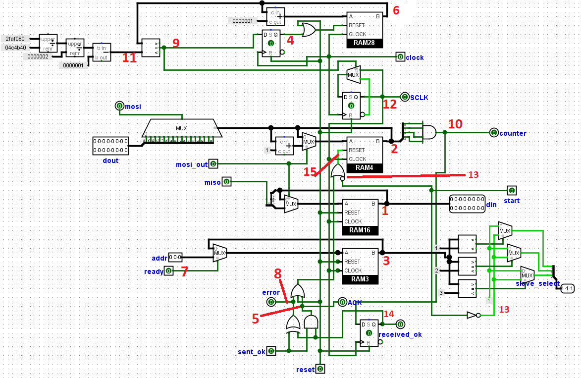
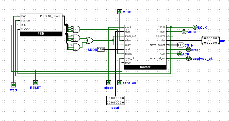
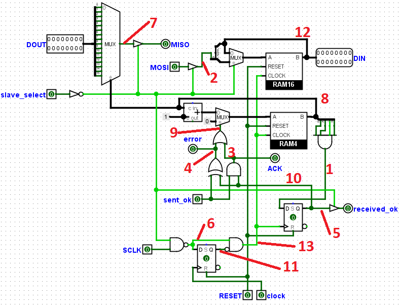
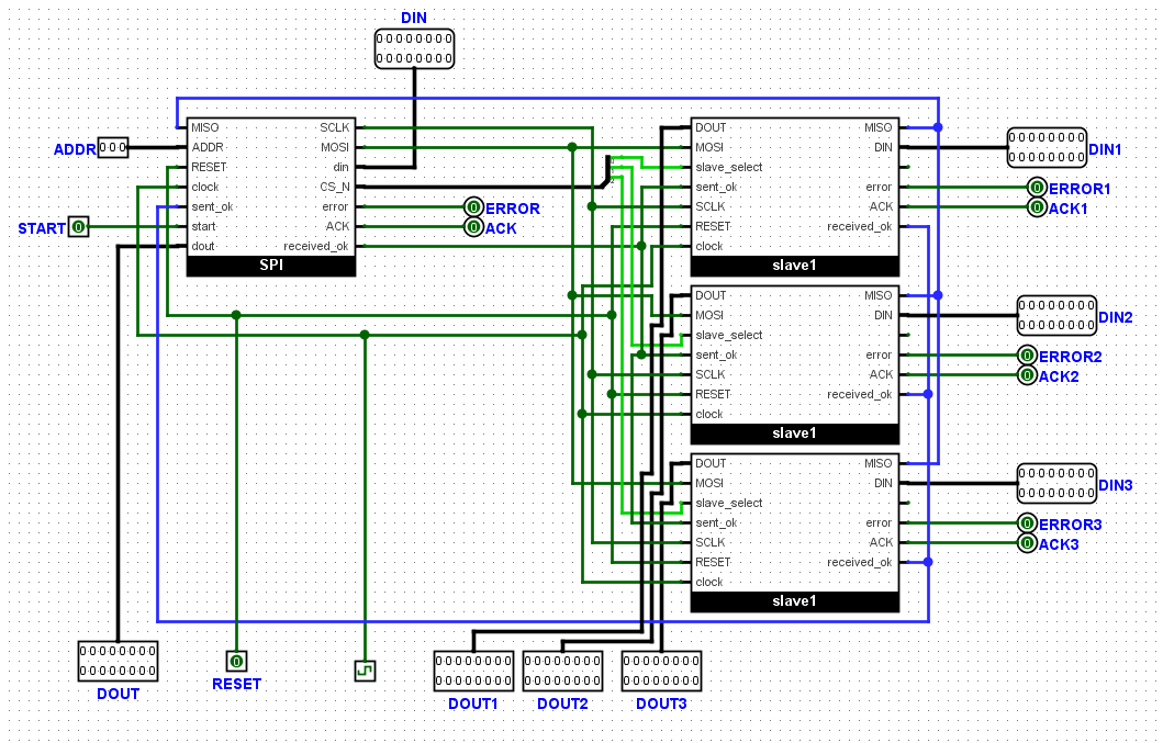
The SPI master consist of two circuits the master state action and the master FSM which will connected together below .


--------------------------------------------------------------------------------
-- PROJECTFPGA.COM
--------------------------------------------------------------------------------
-- NAME:    master_spi
--------------------------------------------------------------------------------
-- AUTHORS: Ezeuko Emmanuel <ezeuko.arinze@projectfpga.com>
--------------------------------------------------------------------------------
-- WEBSITE: https://projectfpga.com/spi
--------------------------------------------------------------------------------
--------------------------------------------------------------------------------
-- SPI MASTER AND SLAVE FOR FPGA
--------------------------------------------------------------------------------
-- Copyright (C) 2020 projectfpga.com
--
-- This source file is free software: you can redistribute it and/or modify
-- it under the terms of the GNU Lesser General Public License as published by
-- the Free Software Foundation, either version 3 of the License, or
-- (at your option) any later version.
--
-- This source file is distributed in the hope that it will be useful,
-- but WITHOUT ANY WARRANTY; without even the implied warranty of
-- MERCHANTABILITY or FITNESS FOR A PARTICULAR PURPOSE.  See the
-- GNU Lesser General Public License for more details.
--
-- You should have received a copy of the GNU Lesser General Public License
-- along with this program.  If not, see <http://www.gnu.org/licenses/>.
--------------------------------------------------------------------------------


library IEEE;
use IEEE.STD_LOGIC_1164.ALL;
use IEEE.NUMERIC_STD.ALL;
use IEEE.MATH_REAL.ALL;
--------------------------------------------------------------------------------
--******************************************************************************
--* This code implements the SPI master protocol                                 *
--* The code uses 3 spi_slaves, you can adjust to any number                     *
--* The spi_slave is in a different VHDL file                                    *                                                   *
--******************************************************************************
--------------------------------------------------------------------------------
entity master_spi is
    Generic (
        CLK_FREQ    : natural := 50e6; -- set system clock frequency in Hz
        SCLK_FREQ   : natural := 5e6;  -- set SPI clock frequency in Hz (condition: SCLK_FREQ <= CLK_FREQ/10)
        SLAVES      : natural := 3    -- count of SPI slaves
    );
    Port (
        CLK               : in  std_logic; -- system clock
        RST               : in  std_logic; -- high active synchronous reset
        -- SPI MASTER INTERFACE
        SCLK             : out std_logic; -- SPI clock
        slave_select     : out std_logic_vector(SLAVES-1 downto 0); -- SPI chip select, active in low
        MOSI             : out std_logic; -- SPI serial data from master to slave
        MISO             : in  std_logic; -- SPI serial data from slave to master
        -- INPUT USER INTERFACE
        ADDR             : in  std_logic_vector(SLAVES-1 downto 0); -- SPI slave address
        DOUT             : in  std_logic_vector(15 downto 0); -- input data for SPI slave
        received_ok      : out  std_logic; --  master acknowledge received data
        sent_ok          : in  std_logic; -- slaves acknowledges received data
        START            : in std_logic; -- marks the beginning os sending data
		  ACK           : out std_logic; -- all is ok
		  error            : out std_logic; -- when error=1, sent_ok and received_ok are not the same
        -- OUTPUT USER INTERFACE
        DIN              : out std_logic_vector(15 downto 0)-- output data from SPI slave
    );
end master_spi;

architecture rtl of master_spi is

signal	 s_ram16                          : std_logic_vector(15 downto 0);
signal	 s_ram4                           : unsigned(3 downto 0);
signal	 s_ram3                           : std_logic_vector(2 downto 0);
signal	 s_ram1_1                         : std_logic;
signal	 s_ACK                            : std_logic;
signal    s_ram28                          : unsigned(WIDTH_CLK_CNT-1 downto 0);
signal	 s_ready                          : std_logic;
signal	 s_error                          : std_logic;
signal	 ticker                           : std_logic;
signal	 counter                          : std_logic;
constant DIVIDER_VALUE                     : integer := (CLK_FREQ/SCLK_FREQ)/2;
signal	 s_sclk                           : std_logic;
signal	 s_sel                            : std_logic;
signal	 s_received_ok                    : std_logic;
signal	 reset_ram4                       : std_logic;


--spi master FSM
type stages is (stage0, stage1, stage2, stage3, stage4);

signal	 stage                            : stages;
 begin

        ticker                      <= '1' when (s_ram28 = DIVIDER_VALUE-1) else '0';
        counter                     <= '1' when (s_ram4 = "1111") else '0';
		  mosi                        <= DOUT(to_integer(unsigned(s_ram4)));
        SCLK                        <= s_sclk;
        DIN                         <=s_ram16;
        s_error                     <= sent_ok xor s_received_ok;
		  error                       <= s_error;
		  s_ACK                       <= sent_ok and s_received_ok;
		  ACK                         <=s_ACK;
		  received_ok                 <= s_received_ok;
		  reset_ram4                  <= s_error or  s_ACK or RST or s_sel;


	sclk_counter : process (RST, CLK)
    begin
	 if RST='1' then
	 s_ram28                          <=(others => '0');
	 s_ram1_1                         <='0';
	 s_sclk                           <='0';


	 elsif rising_edge(CLK) then
	 if (ticker = '1') then
	 s_ram28                         <=(others => '0');
	 s_sclk                          <=not s_sclk;
	 else
	 s_sclk                          <= s_sclk;
	 s_ram28                         <= s_ram28 + 1;

	end if;
	end if;
  end process sclk_counter;

	states: process (RST, S_SCLK)
    begin
	 if reset_ram4='1' then
	 s_ram4                           <=(others => '0');


	 elsif  RST='1' then

	 stage                            <=stage1;
	 s_ram16                          <=(others => '0');
	 s_ram3                           <=(others => '0');
	 s_ram1_1                         <='0';
	 s_received_ok                    <='0';

	 elsif rising_edge(S_SCLK) then
	 s_received_ok                     <=counter ;

	case stage is

    when stage0 =>
	 if (start = '1') then
      stage                           <= stage1;
      else
      stage                           <= stage0;
      end if;

when stage1 =>
   s_ready                           <='1';
	s_ram3                          <=ADDR;
   stage                           <= stage2;


when stage2 =>
	   s_ram4                          <= s_ram4 + 1;
	   s_ram16                         <= s_ram16(14 downto 0) & MISO;
		s_sel                           <= '0';
      if (counter = '1') then
      stage                           <= stage4;
      else
      stage                           <= stage3;
      end if;


when stage3 =>
	   s_ram4                          <= s_ram4 + 1;
	   s_ram16                         <= s_ram16(14 downto 0) & MISO;
		s_sel                           <= '0';
      if (counter = '1') then
      stage                           <= stage4;
      else
      stage                           <= stage2;
      end if;

when stage4 =>

	    if (s_ACK= '1') then
     stage                            <= stage0;
      else
     stage                            <= stage4;
     end if;

 when others =>
       stage                          <= stage0;

        end case;
	end if;
 end process;

     cs_n_g : for i in 1 to SLAVES generate
        cs_n_p : process (s_sel, s_ram3)
        begin
            if (to_integer(unsigned(s_ram3)) = i) then
                slave_select(i-1) <= s_sel;
            else
                slave_select(i-1) <= '1';
            end if;
        end process;
    end generate;


end rtl;


--------------------------------------------------------------------------------
    -- PROJECTFPGA.COM
    --------------------------------------------------------------------------------
    -- NAME:    spi slave
    --------------------------------------------------------------------------------
    -- AUTHORS: Ezeuko Emmanuel <ezeuko.arinze@projectfpga.com>
    --------------------------------------------------------------------------------
    -- WEBSITE: https://projectfpga.com/spi
    --------------------------------------------------------------------------------
    --------------------------------------------------------------------------------
    -- SPI MASTER AND SLAVE FOR FPGA
    --------------------------------------------------------------------------------
    -- Copyright (C) 2020 projectfpga.com
    --
    -- This source file is free software: you can redistribute it and/or modify
    -- it under the terms of the GNU Lesser General Public License as published by
    -- the Free Software Foundation, either version 3 of the License, or
    -- (at your option) any later version.
    --
    -- This source file is distributed in the hope that it will be useful,
    -- but WITHOUT ANY WARRANTY; without even the implied warranty of
    -- MERCHANTABILITY or FITNESS FOR A PARTICULAR PURPOSE.  See the
    -- GNU Lesser General Public License for more details.
    --
    -- You should have received a copy of the GNU Lesser General Public License
    -- along with this program.  If not, see <http://www.gnu.org/licenses/>.
    --------------------------------------------------------------------------------


    library IEEE;
    use IEEE.STD_LOGIC_1164.ALL;
    use IEEE.NUMERIC_STD.ALL;

    -- THE SPI SLAVE MODULE SUPPORT ONLY SPI MODE 0 (CPOL=0, CPHA=0)!!!

    entity slave_spi is
        Port (
            CLK      : in  std_logic; -- system clock
            RST      : in  std_logic; -- high active synchronous reset
            -- SPI SLAVE INTERFACE
            SCLK             : in  std_logic; -- SPI clock
            slave_select     : in  std_logic; -- SPI chip select, active in low
            MOSI             : in  std_logic; -- SPI serial data from master to slave
            MISO             : out std_logic; -- SPI serial data from slave to master
            -- USER INTERFACE
            DOUT      : in  std_logic_vector(15 downto 0); -- input data from SPI slave
            DIN       : out std_logic_vector(15 downto 0); -- output data from SPI master TO SLAVE
            received_ok      : out  std_logic; --  master acknowledge received data
            sent_ok          : in  std_logic; -- slaves acknowledges received data
    		  ACK           : out std_logic; -- all is ok
    		  error            : out std_logic -- when error=1, sent_ok and received_ok are not the same
        );
    end slave_spi;

    architecture RTL of slave_spi is

        signal counter            : std_logic;
    	 signal mosi_in            : std_logic;
        signal s_ACK              : std_logic;
        signal s_error            : std_logic;
        signal s_received_ok      : std_logic;
        signal s_ram1_2_data      : std_logic;
        signal s_out              : std_logic;
        signal s_ram4             : unsigned(3 downto 0);
        signal reset_ram4         : std_logic;
        signal s_ram1_1           : std_logic;
        signal s_ram1_2           : std_logic;
        signal s_ram16            : std_logic_vector(15 downto 0);
        signal s_SCLK             : std_logic;


    begin

     counter                          <= '1' when (s_ram4 = "1111") else '0';
     s_ram1_2_data                    <= SCLK nand not slave_select;
     s_SCLK                           <=  not s_ram1_2_data and s_ram1_2;
     s_out                            <= DOUT(to_integer(unsigned(s_ram4)));
     DIN                              <= s_ram16;

            s_error                     <= sent_ok xor s_received_ok;
    		  error                       <= s_error;
    		  s_ACK                       <= sent_ok and s_received_ok;
    		  ACK                         <=s_ACK;

    		  reset_ram4                  <= s_error or  s_ACK;

    tri_state_buffer : process (slave_select)
    begin
         if (slave_select = '1') then
           mosi_in                          <= 'Z';
           MISO                             <= 'Z';
           received_ok                      <= 'Z';
     else

           MISO                             <=s_out;
           mosi_in                          <= MOSI;
    		 received_ok                      <= s_received_ok;
    end if;
    end process tri_state_buffer;

     clocking: process (RST, CLK)
        begin
    	  if (RST = '1') then
               s_ram1_2                  <= '0';
            elsif (rising_edge(CLK)) then
    		     s_ram1_2                  <= s_ram1_2_data;

    end if;
    end process clocking;

     spi: process (RST, s_SCLK)
        begin
    	  if (RST = '1') then
    	 s_ram16                          <=(others => '0');
    	 s_ram4                           <=(others => '0');
        s_ram1_1                         <= '0';
            elsif (rising_edge(s_SCLK)) then
    			  s_received_ok             <= counter;
    			   if(slave_select = '1') then
    				s_ram16                  <= s_ram16(14 downto 0) & MOSI;
    				end if;
    				if( reset_ram4 = '1' ) then
    				s_ram4                   <=(others => '0');
    				else
    				s_ram4                   <= s_ram4 +1;

    				end if;
               			end if;


    end process spi;

    end rtl;
