SDRAM is a CMOS high-speed, dynamic random access memory (DRAM) and it is configured as a quad-bank Dynamic RAM internally with a synchronous interface means that all signals are registered on the falling or rising edge of the clock signal.
Accessing of the data from a memory location begins with an ACTIVE command from the interpreter and it is then followed by a READ/WRITE command. In general memory is represented in banks, rows and column. To point to a location in the memory these three are mandatory. The ACTIVE command signal along with registered address bits point to the specific bank and row to be accessed. And column is given by READ/WRITE signal along with the registered address bits that shall point to a location for burst access.
The interface uses double pumping means transferring data on both the rising as well as falling edges of the clock signal to lower the clock frequency. One of the major uses of keeping the clock frequency down is that it reduces the signal integrity requirements connecting the memory to the controller on the circuit board. The "double data rate" means with a certain clock frequency a DDR SDRAM achieves virtually double the bandwidth of a SDR SDRAM working at the same clock frequency due to double pumping at the interface of memory controller.
Because of the internal bus width is two times the external bus width; DDR SDRAM achieves a data output rate that is almost twice the data rate of the internal bus. Double data rate (DDR) SDRAM—SDRAM, latches command information on the positive or rising edge of the clock; data is driven or latched on both the positive and negative edges of the clock rather than just the rising edge. This method doubles the data throughput rate without an increase in frequency.
DDR SDRAM utilizes a differential clock (CLK, CLK’) and data strobe signal DQS for high-speed burst mode data transfer. DQS is synchronized with clock signal, and data input and output (DQ) is synchronized with both the positive and negative of the CLK. A bidirectional data strobe (DQS) is transmitted along with data. DQS is used to capture data at the receiver. DQS is a strobe signal transmitted by the memory controller during WRITE operation and by the DDR SDRAM during READ mode. The read/write accesses to the DDR SDRAM are burst mechanism based, means more than one location data are read at a time and usually accessing starts at a specified location and continue to fetch data for required number of locations.
DRAM reads are destructive, meaning the data in the row of memory cells are destroyed in the read operation. Therefore, the row data need to be written back into the same row after the completion of a read or write operation on that row. This operation is called precharge and is the last operation on a row. It must be done before accessing a new row and is referred to as closing an open row.
A DRAM row is called a memory page and once the row is opened you can access multiple sequential or different column addresses in that row. This increases memory access speed and reduces memory latency by not having to resend the row address to the DRAM when accessing memory cells in the same memory page. As a result, the row address is the computer’s higher order address bits and the column address is the lower order address bits. Since the row and column addresses are sent at different times, the row address and the column address are multiplexed on the same DRAM pins in order to reduce package pin count, cost and size. Typically the size of the row address is larger than the column address because the power usage is related to the number of columns.
Early DRAMs had control signals such as RAS# (Row Address Select active low) and CAS# (Column Address Select active low) to select the row and column addressing operation being performed. Additional DRAM control signals include WE# (Write Enable active low) for selecting write or read operation, CS# (Chip Select active low) for selecting the DRAM and OE# (output enable active low). The early DRAMs had control signals that were asynchronous and had various timing specifications covering their sequence and time relationships to determine the DRAM operating mode.
The early DRAMs read cycle had four steps. First, RAS# goes low with a row address on the address bus. Secondly, CAS# goes low with a column address on the address bus. Third, OE# goes low and read data appears on DQ data pins. The time from the first step to the third step when data is available on DQ pins is called latency. The last step is RAS#, CAS# and OE# going high (inactive) and waiting for the internal precharge operation to complete restoration of the row data after the destructive read. The time from the first step to completion of the last step is the memory cycle time. Signal timing of the above signals is related to the sequence of edges and is asynchronous. There are no synchronous clock operations with these early DRAMs.
DDR SDRAM
DDR (Double Data Rate) SDRAMs increased the memory data rate performance by increasing clock rates, bursting of data and transferring two data bits per clock cycle.
DDR SDRAMs burst multiple memory locations in a single read or single write command. A read memory operation entails sending an Activate command followed by a Read command.
The memory responds after its latency with a burst of two, four, or eight memory locations at a data rate of two memory locations per clock cycle. Therefore,
four memory locations are read from or written to in two consecutive clock cycles.
DDR SDRAMs have multiple banks to provide multiple interleaved memory access, which increases memory bandwidth. A bank is one array of memory, two banks are two arrays of memory, four banks are four arrays of memory, etc (See Figure 3). Four banks require two bits for bank address (BA0 & BA1).
For example, a DDR SDRAM with four banks operates in the following manner. First, an Activate command opens a row in the first bank. A second Activate command opens a row in the second bank. Now any combinations of Read or Write commands can be sent to either the first bank or the second bank with their open rows. When Read and Write operations on the bank are completed, a Precharge command closes the row and the bank is ready for an Activate command to open a new row.
DDR2 SDRAM
DDR2 SDRAM has several improvements over DDR SDRAM. DDR2 SDRAM clock rates are higher, thus increasing the memory data rates. Signal integrity becomes more important
for reliable memory operation as the clock rates increase. As clock rates increase, signal traces on the circuit boards become transmission lines and proper layout
and termination at the end of the signal traces becomes more important.
Termination of the address, clock and command signals are somewhat straightforward because these signals are unidirectional and are terminated on the circuit boards. The data signals and data strobes are bidirectional. The memory controller hub drives them during a write operation and the DDR2 SDRAM drives them during a read operation. To add to the complexity, multiple DDR2 SDRAMs are connected to the same data signals and data strobes. These multiple DDR2 SDRAMs can be on the same DIMM and on different DIMMs in the memory system. As a result, the data and data strobe drivers and receivers are constantly changing depending upon the read/write operation and which DDR2 SDRAM is being accessed.
DDR2 SDRAM improves the signal integrity of data signals and data strobes by providing ODT (On-Die Termination), an ODT signal to enable the on-die termination and the ability to program the on-die termination values (75 ohms,150 ohms, etc.) with the DDR2 SDRAM extended mode register.
The on-die termination value and operation is controlled by the memory controller hub and are a function of a DDR2 SDRAM DIMM’s location and type of memory operation (reads or writes). ODT operation results in better signal integrity by creating a larger eye diagram for the data valid window with increased voltage margins, increased slew rates, reduced overshoot and reduced ISI (Inter-Symbol Interference).
A new feature introduced with DDR2 SDRAM is additive latency, which provides the memory controller hub the flexibility to send the Read and Write commands sooner after the Activate command. This optimizes memory throughput and is configured by programming the additional latency using the DDR2 SDRAM extended mode register.
DDR3 SDRAM
Both DDR2 and DDR3 SDRAMs have four mode registers. DDR2 defined the first two mode registers while the other two were reserved for future use.
DDR3 uses all four mode registers. One significant difference is DDR2 mode registers defined CAS latency for read operation and the write latency was one less the
mode register read latency setting. DDR3 mode registers have unique settings for both the CAS read latency and write latency.
DDR3 SDRAM uses 8n prefetch architecture which transfers 8 data words in 4 clock cycles. DDR2 SDRAM uses 4n prefetch architecture which transfers 4 data words in 2 clock cycles.
The DDR3 SDRAM mode registers are programmed to support the on the fly burst chop, which shortens the transfer of 8 data words to 4 data words by setting the address line 12 low during a read or write command. On the fly burst chop is similar in concept to the read and write auto-precharge function of the address line 10 in both DDR2 and DDR3 SDRAMs.
Other noteworthy DDR3 SDRAM attributes include the data strobes DQS which are differential, whereas DDR2 SDRAM data strobes could be programmed by the mode register to be single-ended or differential. DDR3 SDRAM also has a new pin which is the active low asynchronous RESET# pin, which will improve system stability by putting the SDRAM in a known state regardless of the current state. DDR3 SDRAM uses the same type of FBGA packages as DDR2 SDRAM.
DDR3 DIMMs have the terminations for the commands, clock and address on the DIMM. Memory systems using DDR2 DIMM terminate the commands, clock and address on the motherboard. The DDR3 DIMM terminations on the DIMM allow a fly-by topology where each command, clock and address pin on the SDRAM is connected to a single trace which is terminated at the trace end on the DIMM. This improves the signal integrity and results in faster operation than the DDR2 DIMM tree structure.
The fly-by topology introduces a new write leveling feature of DDR3 SDRAM for the memory controller to account for the timing skew between the clock CK and data strobes DQS during writes. The DDR3 DIMM is keyed differently than the DDR2 DIMM to prevent the wrong DIMM being plugged into the motherboard.


SDRAMs have a multi-bank architecture and is organized in banks, rows and columns.
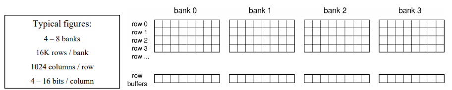
Many chips are combined on a memory module to increase the word width. This is called the memory configuration.
The requested row is activated and copied to the row buffer of the corresponding bank.

The row is precharged and stored back into the memory array.

The capacitor is leaking and needs to be periodically refreshed in order not to loose its data.
• All banks must be precharged when a refresh command is issued.
• A DDR2 memory needes to be refreshed once every 64 ms.