Digital to Analog Converter Overview
the Digital to Analog Converter (DAC) is an interface between the digital signal processing system and the analog world. It is a device that converts digital signals
to analog signals (voltage levels, current levels or electric charge).
Connecting digital circuitry to sensor devices is simple if the sensor devices are inherently digital themselves. Switches, relays, and encoders are easily interfaced with gate circuits due to the on/off nature of their signals.
However, when analog devices are involved, interfacing becomes much more complex. What is needed is a way to electronically translate analog signals into digital (binary) quantities, and vice versa. An analog-to-digital converter, or ADC, performs the former task while a digital-to-analog converter, or DAC, performs the latter.
Digital to Analog Data Conversion Tools
Types of DAC
1. Binary Weighted Resistor
Utilizes a summing op-amp circuit.
Weighted resistors are used to distinguish each bit from the most significant to the least significant
Transistors are used to switch between Vref and ground (bit high or low)
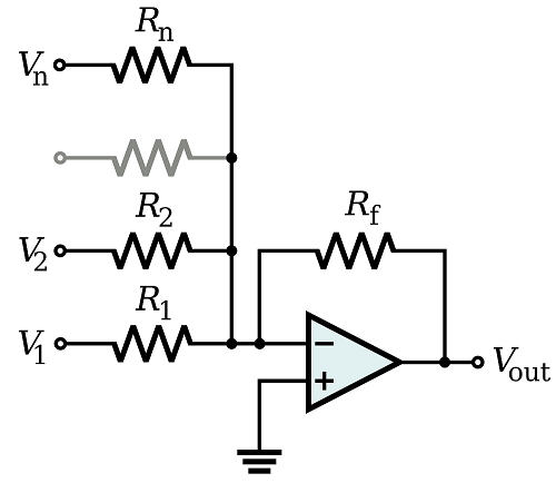
If you recall, the classic inverting summing circuit is an operational amplifier using negative feedback for controlled gain, with several voltage inputs and one voltage output. The output voltage is the inverted (opposite polarity) sum of all input voltages.
For a simple inverting summing circuit, all resistors must be of equal value. If any of the input resistors were different, the input voltages would have different degrees of effect on the output, and the output voltage would not be a true sum.
Voltages V1 through Vn are either Vref if corresponding bit is high or ground if corresponding bit is low.
V1 is most significant bit (MSB) Vn is least significant bit (LSB)
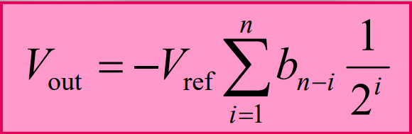
Vout = -IRf = -Rf ( V1/R +V2/2R + V3/4R +.......Vn/2n-1R )
If Rf = R/2
Vout = -IRf = -Rf ( V1/2 +V2/4 + V3/8 +.......Vn/2n )
For example, a 4-Bit converter yields
Vout = -Vref
( b3 1/2
+ b2 1/4
+ b1 1 /8
+ b0 1 /16)
Where b3, b2, b1, b0 Corresponds to
Bit 3, 2, 1 and 0 respectively.
If we wish to expand the resolution of this DAC (add more bits to the input), all we need to do is add more input resistors, holding to the same power-of-two sequence of values:
Example 1
Calculate the value of Vo, of a 4-bit weighted –resistor DAC, where Vref = 5V, R = 1kΩ, Rf = 470 Ω, and digital input of 1010 is applied.
Solution:
Vo = -Rf[Vref
( b3 1/R
+ b2 1/2R
+ b1 1 /4R
+ b0 1 /8R)]
-Rf[Vref ( b3 8/8R + b2 4/8R + b1 2 /8R + b0 1 /8R)]
= 470 *5[(8*1) + (4*0) + (2*1) + (1*0)]/8*1000 = -2.973V
Binary Weighted Resistor Advantages
Simple Construction/Analysis
And Fast Conversion
Disadvantages
1. Requires large range of resistors (2000:1 for 12- bit DAC) with necessary high precision for low resistors
2. Requires low switch resistances in transistors
3. Can be expensive. Therefore, usually limited to 8- bit resolution.
2. Summing Amplifier Converter
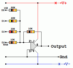
In this diagram if the binary input is 0101, using the summing amplifier formula ...
Vout = -10( 0 / 10 + 5 / 20 + 0 / 40 + 5 / 80 ) = 250 / 80 = -3.125 Volts
Resolution
Resolution is the size of the voltage steps as the digital data is incremented (add one) or decremented (subtract one).
0.625 Volts is the size of the smallest step. This is the resolution of the DAC.
R/2R DAC
R-2R Digital-to-Analogue Converter, or DAC, is a data converter which use two precision resistor to convert a digital binary number into an analogue output signal
proportional to the value of the digital number
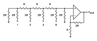
Starting from the left hand side and using the simplified equation for two parallel resistors and series resistors, we can find the equivalent resistance of the ladder network as:
Resistors R1 and R2 are in "parallel" with each other but in "series" with resistor R3 . Then we can Resolve them in parallel to be in series with resistor R3 .
R1&2 = R1 * R2 / R1 + R2 = 2R* 2R/2R + 2R
=4R2/4R = R
Let R1&2 = Ra
Therefore Ra = R3 equal to R.
Adding Ra and R3 in series is equivalent to2R
Now we can see that the equivalent resistance "2R" is in parallel with R4 with the parallel combination in series with R5.
Resolving 2R in parallel with R4 = R
Adding it to R5 in series is equivalent to 2R
The same repeats till R8.
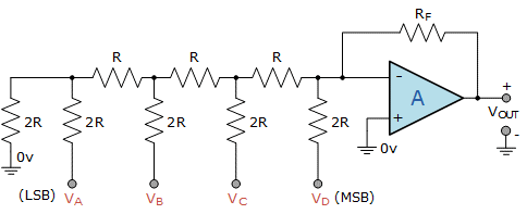
From voltage divider rule :
V3 = [R/R+R] V2 = 1/2 (V2).
Likewise,
V2 = 1/2 * V1
V1 = 1/2 * Vref
Vout = -IR
Expressing them in terms of Vref
V3 = 1/8 * Vref
V2 = 1/4 * Vref
V1 = 1/2 * Vref
Therefore, each voltage is half of the preceeding node.
For a 4-bit R-2R Ladder network , we will also have
V4 = 1/16 * Vref
Vout = -R(
B3Vref/2R +
B2Vref/4R +
B1Vref/8R +
B0Vref/16R
)
= -Vref(
B31/2 +
B21/4 +
B11/8 +
B01/16
)
For general n-Bit R-2R Ladder or Binary Weighted Resister DAC
Advantages
Only two resistor values (R and 2R) and Does not require high precision resistors
Disadvantage
Lower conversion speed than binary weighted DAC
Example 1
For the circuit shown above with Vref = 5V and R = Rf = 2KOhms, calculate the output voltage V0 for an input code word 1110.
Vo = -Vref * [(8b3 + 4b2 + 2b1 +1b0) / (16)]
Vo = -5 [(8x1)+(4x1)+(2x1)+(1x0) /16]
= - 5 * (8 + 4 + 2) / 16
= - 4.375 volts
Example 2
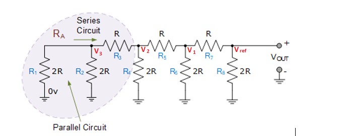
Find the output voltage for an R-2R DAC. The digital input is 110.
R = 15K, 2R = 30K, Rf= 15K, Vref= 5V
Iin = Vref/R = 5V/15KOhms = 0.333mA
I2 = Vref/2R = 5V/30 KOhms = 0.1667 mA
I1 = I2/2 = 0.1667mA/2 = 0.833 mA = 83.33 mA
Io = I1 / 2 = 0.0833mA / 2 = 0.04166mA = 41.66mA
IT = I2 + I1 = 0.1667mA + 0.0833mA = 0.25003 mA
Vo = -ITRf = -0.25003mA * 15 KOhms = -3.75045 V
Example 3
Output voltage range: This is the difference between the maximum and minimum output voltages expressed in volts.
Calculate the output voltage range of a 4-bit DAC if the output voltage is +4.5V for an input of 0000 and +7.5V for an input of 1111.
Output voltage range = 7.5 - 4.5 = 3.0V
Example 4
Resolution: It is the smallest possible change in the analog output as a result of the change in digital input. Resolution should be as high as possible.
A 4 bit D/A converter have an output range of 0 to 1.5 V. Define its resolution.
Given, n = 4 = number of bits
Full scale output, VOFS = 1.5V
2n =24 = 16
Thus the output voltage can have 16 different values including zero.
Resolution: R = VOFS /2n-1 = 1.5/16-1 = 1.5/15 = 100mV/LSB.
Thus, an input change of 1 LSB changes the output by 100 mV.
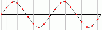
Sampling a Signal
The carrier signal used to carry data or the clock frequency used to sample data needs to be on a frequency at least double the highest data/music/voice frequency.
The Nyquist Frequency also known as the critical frequency is the highest data/music/voice frequency that can be transmitted. This is half the sampling or carrier frequency.
As the transmission frequency increases, the amount of sampled data that can be encoded also increases. For digital transmissions, UHF and Microwave are preferred over the LF, MF and VHF bands. Fibre-optic is even better due to the exceedingly high frequency of light.
The frequency of light is in the region of 1014 Hz. Theoretically data rates of half this figure should be possible if the light emitting and detecting devices and the fibres could ever be made good enough.
Plenty of Samples - This will work - The original signal can be re-constructed fairly well
Sample and Hold Circuit
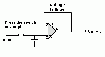
Sample and Hold circuits are used to "remember" an analogue voltage for a time period long enough to process the sample. For example if an analogue signal is being converted to digital, the signal must be held for the duration of the conversion.
The simplest circuit could be a single capacitor. This would be satisfactory if there was no capacitor leakage current and the ADC input had a very high input resistance. In addition, there would need to be a way to disconnect the input while the sample was being held.
A better solution is to use a capacitor with a voltage follower. The voltage follower has the required high input resistance and it can drive the ADC input which need not have a high input resistance.
While the switch is open, the capacitor voltage will remain constant assuming there is no leakage current through the capacitor or the op' amp'.
When the switch is closed, the capacitor will rapidly charge to match the input voltage.
For a real life application, the input switch needs to be digitally controlled.
Analogue Switch chips are available. While active, the switch is closed. In the "off" state, the analogue chip has a high output resistance.
This effectively disconnects the analogue switch. This ability to disconnect is similar to tristate logic chips which do the same thing.
The CD4066B chip is suitable. It contains four analogue switches. When active, the input is copied to the output. When disabled, the leakage current is about 10 pA (pico-amps).
Analog to digital converters
1. Flash Analog to Digital Converter
Flash analog-to-digital converters, also known as parallel ADCs, are the fastest way to convert an analog signal to a digital signal. Flash ADCs are ideal for applications
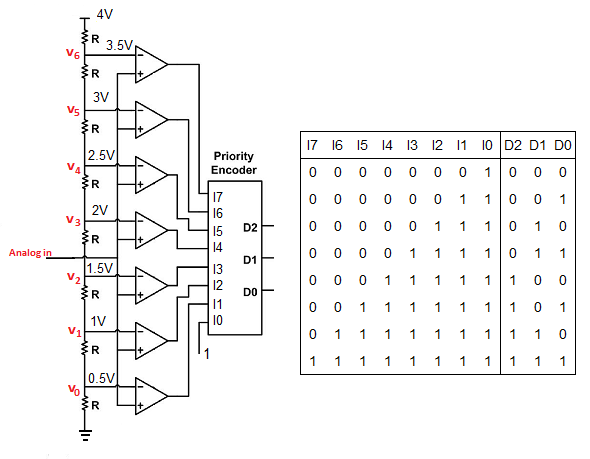
requiring very large bandwidth, but they consume more power and much bigger in size than other ADC architectures. A Flash converter requires a huge number of comparators
compared to other ADCs, especially as the resolution increases. A Flash converter requires 2n-1 comparators for an n-bit conversion.
As the analog input voltage exceeds the reference voltage at each comparator, the comparator outputs will sequentially saturate to a high state. The priority encoder generates a binary number based on the highest-order active input, ignoring all other active inputs. An N-bit flash ADC consists of 2 powered N-1 comparators and contains 2 powered N number of matched resistors and a priority encoder.The circuit below has Vref=4V, The analog input is compared on seven different comparators with different levels (V 0, V 1, V2,V3, V4, V5, V6). The voltage levels decrease down the line. From KVL:
Assuming all resistors are equal.
V 0= V T( R0/ R T) = 4*(1/8) = 0.5V
This is also equal to the resolution.
Therefore V 1, V2,V3, V4, V5, V6, V ref = 1v, 1.5v, 2v, 2.5v, 3v, 3.5, 4v respectively.
V 1= V T( R1/ R T) = 4*(2/8) = 1V
V 2= V T( R2/ R T) = 4*(3/8) = 1.5V
V 3= V T( R3/ R T) = 4*(4/8) = 2V
V 4= V T( R4/ R T) = 4*(5/8) = 2.5V
V 5= V T( R5/ R T) = 4*(6/8) = 3V
V 6= V T( R6/ R T) = 4*(7/8) = 3.5V
V ref= V T( RT/ R T) = 4*(8/8) = 4V
The priority encoder chart is also given, Starting from I0 to I7. The number of comparators that turns determines the digital output. The number of comparators turn on from i0 to i7 depending on the value of the analog input. The block diagram for the concept is provided below:
Another design of the flash ADC. For this particular application, a regular priority encoder with all its inherent complexity isn't necessary. Due to the nature of the sequential comparator output states (each comparator saturating "high" in sequence from lowest to highest), the same "highest-order-input selection" effect may be realized through a set of Exclusive-OR gates, allowing the use of a simpler, non-priority encoder:
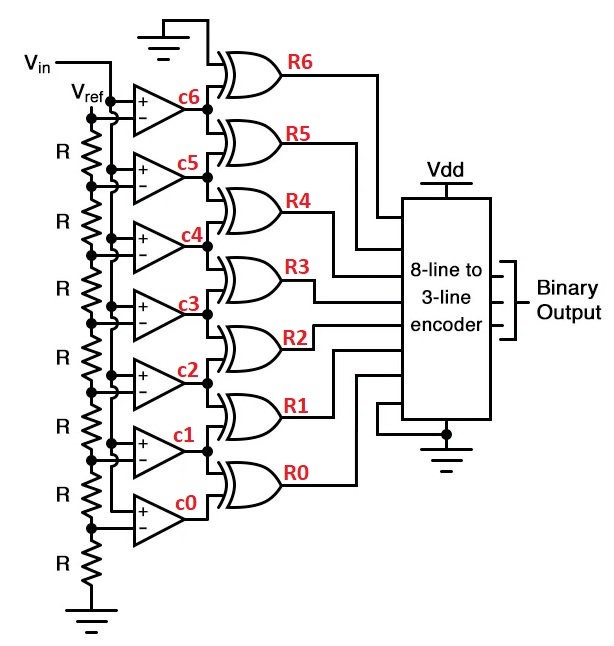
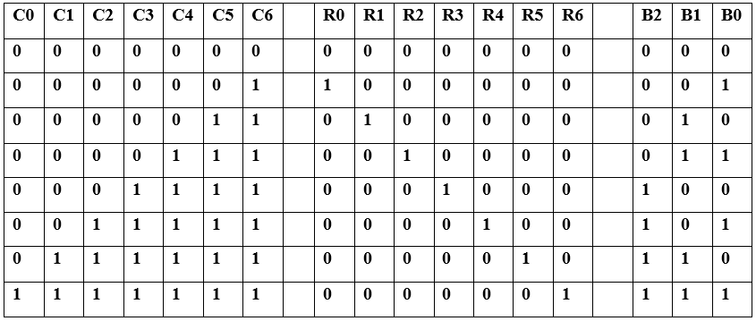
The chart for Comparator output, EX-OR gate output and decoder output is given below.
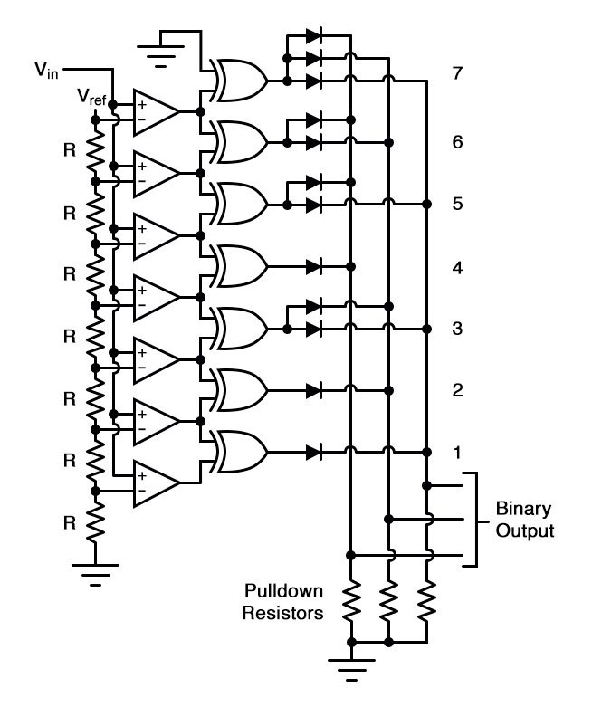
And, of course, the encoder circuit itself can be made from a matrix of diodes, demonstrating just how simply this converter design may be constructed:
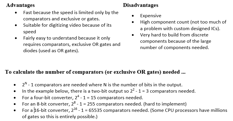
Not only is the flash converter the simplest in terms of operational theory, but it is the most efficient of the ADC technologies in terms of speed, being limited only in comparator and gate propagation delays. Unfortunately, it is the most component-intensive for any given number of output bits.
This three-bit flash ADC requires seven comparators. A four-bit version would require 15 comparators. With each additional output bit, the number of required comparators doubles.
Considering that eight bits is generally considered the minimum necessary for any practical ADC (255 comparators needed!), the flash methodology quickly shows its weakness. An additional advantage of the flash converter, often overlooked, is the ability for it to produce a non-linear output.
With equal-value resistors in the reference voltage divider network, each successive binary count represents the same amount of analog signal increase, providing a proportional response. For special applications, however, the resistor values in the divider network may be made non-equal.
This gives the ADC a custom, nonlinear response to the analog input signal. No other ADC design is able to grant this signal-conditioning behavior with just a few component value changes.
2. Digital Ramp Analog to Digital Converter (ADC)
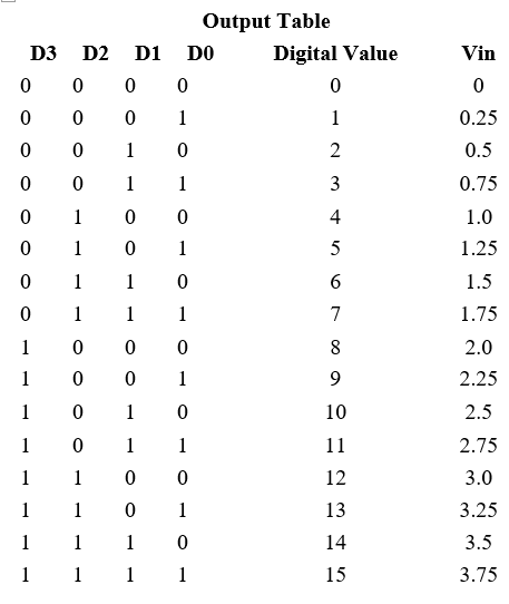
The Digital Ramp ADC is also known as a counter-type ADC. It uses a binary counter as the register and allows the clock to increment the counter one step at a time until Vo > V+.
Circuit shown is a 4 bit Digital Ramp ADC
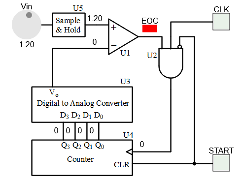
Circuit Operation
Notes:
Ramp ADC Problems
Typical ADC Chips
All the components above are built into one chip. This has pins to ...
3. Successive Approximation ADC
One method of addressing the digital ramp ADC’s shortcomings is the so-called successive-approximation ADC. The only change in this design is a very special counter circuit known
as a successive-approximation register.
Instead of counting up in binary sequence, this register counts by trying all values of bits starting with the most-significant bit and finishing at the least-significant bit. Throughout the count process, the register monitors the comparator’s output to see if the binary count is less than or greater than the analog signal input, adjusting the bit values accordingly.
The way the register counts is identical to the "trial-and-fit" method of decimal-to-binary conversion, whereby different values of bits are tried from MSB to LSB to get a binary number that equals the original decimal number. The advantage to this counting strategy is much faster results: the DAC output converges on the analog signal input in much larger steps than with the 0-to-full count sequence of a regular counter. the circuit looks like this:
The successive-approximation analog-to-digital converter circuit typically consists of four chief subcircuits:
1. A sample-and-hold circuit to acquire the input voltage Vin.
2. An analog voltage comparator that compares Vin to the output of the internal DAC and outputs the result of the comparison to the successive-approximation register (SAR).
3. A successive-approximation register subcircuit designed to supply an approximate digital code of Vin to the internal DAC.
4. An internal reference DAC that, for comparison with Vref, supplies the comparator with an analog voltage equal to the digital code output of the SARin.
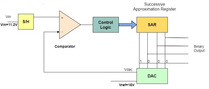
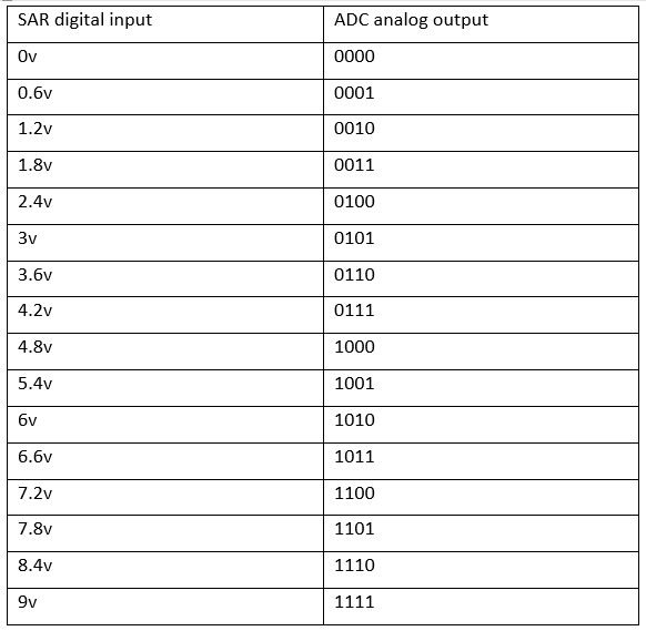
Assuming 9v Reference voltage .
Resolution for 4 bit ADC = 9/15 =0.6V
The chart below shows the SAR digital input and the equivalent ADC analog output
.
Algorithm of a 4-bit successive-approximation ADC
It should be noted that the SAR is generally capable of outputting the binary number in serial (one bit at a time) format, thus eliminating the need for a shift register.
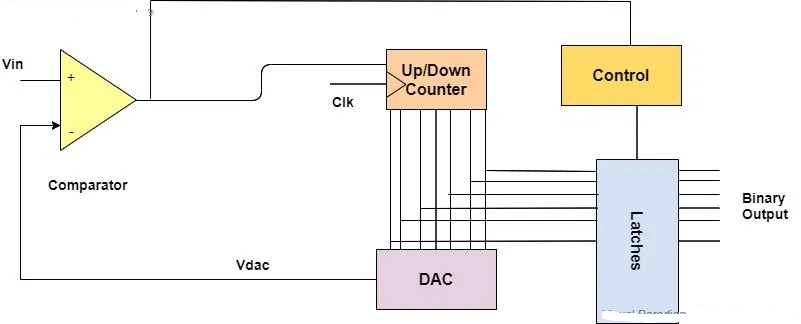
4. Tracking ADC
The tracking type analog to digital converter consists of a comparator, control circuit, an up-down counter, a digital to analog converter, and an output latch circuit that gives
out the final binary outputs.
A third variation on the counter-DAC-based converter theme is, in my estimation, the most elegant. Instead of a regular "up" counter driving the DAC, this circuit uses an up/down counter.
The counter is continuously clocked, and the up/down control line is driven by the output of the comparator. So, when the analog input signal exceeds the DAC output, the counter goes into the "count up" mode.
When the DAC output exceeds the analog input, the counter switches into the "count down" mode. Either way, the DAC output always counts in the proper direction to track the input signal.
Tracking Type ADC Working
The comparator receives two voltages i.e. input voltage and the reference voltage. The input analog voltage is applied to the non-inverting end of the comparator whereas the
reference voltage is applied to the negative or inverting end of the comparator. This reference voltage is basically the output of the digital to analog converter that gets
compared with the given input voltage and determines the state of the comparator.
If Vin > Vdac
When the respective analog to digital converter is powered on, the output of the digital to analog converter is zero. When this is compared with the applied voltage, the
comparator gets high and the counter starts its counting from zero onwards. It means that it starts counting in the upward direction. In return, the output of the digital
to analog converter starts to increase slowly.
If Vin < Vdac
But when the continuous input voltage is less than the output of the digital to analog converter, the comparator goes from high to low state at that particular time.
This enables the up-down counter to start its counting in the reverse direction that is in the down direction instead of resetting itself just like the counter type ADC.
Once again when the output of the digital to analog converter becomes greater than the input voltage, the comparator becomes high and the counter enters up count mode and vice versa the counter enters the down count mode. The condition for whether the counter counts in an upward or downward direction depends on the input voltage and the process keeps on repeating.
This analog to digital converter keeps the track of the input voltage consistently for its functionality therefore it is called a Tracking type analog to digital converter.
Output Latching
The output of the counter is latched whenever the comparator transits its output. It means that every time when the output of the comparator transitions from high to low or low
to high state then the binary output of the up-down counter is latched.
Conversion Time
Here is the visual pattern of the output of the digital to analog converter:
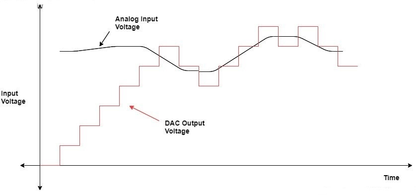
The graph shows that in the beginning, the output of the digital to analog converter was increasing gradually until it reached and tracked the input voltage.
The maximum conversion time at this point
Tc(max) = (2^N-1)Tclk
Where N is the number of bits of analog to digital converter and Tclk is the duration of the clock pulse.
This depicts that when the changer in the input voltage becomes equal to the full-scale voltage of the digital to analog converter the up-down counter moves from all zeros to
all ones (0000--->1111) and from all ones to all zeros (1111---->0000).
Notice how no shift register is needed to buffer the binary count at the end of a cycle. Since the counter’s output continuously tracks the input (rather than counting to meet
the input and then resetting back to zero), the binary output is legitimately updated with every clock pulse.
An advantage of this converter circuit is speed, since the counter never has to reset.
5. Delta-Sigma ADC
One of the more advanced ADC technologies is the so-called delta-sigma, or ΔΣ (using the proper Greek letter notation). In mathematics and physics, the capital Greek letter delta
(Δ) represents difference or change, while the capital letter sigma (Σ) represents summation: the adding of multiple terms together. Sometimes this converter is referred to by the
same Greek letters in reverse order: sigma-delta, or ΣΔ.
In a ΔΣ converter, the analog input voltage signal is connected to the input of an integrator, producing a voltage rate-of-change, or slope, at the output corresponding to input magnitude. This ramping voltage is then compared against ground potential (0 volts) by a comparator.
The comparator acts as a sort of 1-bit ADC, producing 1 bit of output ("high" or "low") depending on whether the integrator output is positive or negative. The comparator’s output is then latched through a D-type flip-flop clocked at a high frequency, and fed back to another input channel on the integrator, to drive the integrator in the direction of a 0 volt output. The basic circuit looks like this:
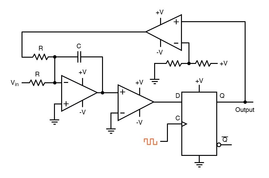
The leftmost op-amp is the (summing) integrator. The next op-amp the integrator feeds into is the comparator, or 1-bit ADC. Next comes the D-type flip-flop, which latches the comparator’s output at every clock pulse, sending either a "high" or "low" signal to the next comparator at the top of the circuit.
This final comparator is necessary to convert the single-polarity 0V / 5V logic level output voltage of the flip-flop into a +V / -V voltage signal to be fed back to the integrator. If the integrator output is positive, the first comparator will output a "high" signal to the D input of the flip-flop.
At the next clock pulse, this "high" signal will be output from the Q line into the noninverting input of the last comparator. This last comparator, seeing an input voltage greater than the threshold voltage of 1/2 +V, saturates in a positive direction, sending a full +V signal to the other input of the integrator.
This +V feedback signal tends to drive the integrator output in a negative direction. If that output voltage ever becomes negative, the feedback loop will send a corrective signal (-V) back around to the top input of the integrator to drive it in a positive direction.
This is the delta-sigma concept in action: the first comparator senses a difference (Δ) between the integrator output and zero volts. The integrator sums (Σ) the comparator’s output with the analog input signal.